Sn-based brazing filler metal capable of realizing vertical stacking of chips and bonding method of Sn-based brazing filler metal

A vertical stacking, chip technology, applied in welding/cutting media/materials, nanotechnology for materials and surface science, welding media, etc., can solve problems such as inapplicability to high-density packaging of three-dimensional packaging electronic devices, different performance, etc. Achieve the effect of meeting high reliability requirements, high strength and service life, and high mechanical properties of solder joints

Pending Publication Date: 2021-11-30
XUZHOU NORMAL UNIVERSITY
View PDF2 Cites 1 Cited by
  • Summary
  • Abstract
  • Description
  • Claims
  • Application Information

AI Technical Summary

Problems solved by technology

The Sn-based lead-free solder disclosed in U.S. Patent US10434608B2 includes (1.2-4.5%) Ag, (0.25-0.75%) Cu, (1.0-5.8%) Bi, (0.01-0.15%) Ni, and the rest is Sn. By optimizing the content of alloying elements, the wettability of solder, the shear performance of solder joints and the thermal fatigue resistance are enhanced to a certain extent. This patent is mainly aimed at conventional SMT (Surface Mounted Technology) solder joints. The solder joints are composed of intermetallic Composed of compound layer and solder matrix, conventional SMT solder joints occupy most of the solder joints due to the short soldering time, but for tiny solder joints in high-density packaging and three-dimensional packaging, intermetallic compounds occupy Most of the solder joints are removed, which leads to completely different performance, so this patented solder is not suitable for high-density packaging and three-dimensional packaging electronic device

Method used


Image

  • Sn-based brazing filler metal capable of realizing vertical stacking of chips and bonding method of Sn-based brazing filler metal
  • Sn-based brazing filler metal capable of realizing vertical stacking of chips and bonding method of Sn-based brazing filler metal
  • Sn-based brazing filler metal capable of realizing vertical stacking of chips and bonding method of Sn-based brazing filler metal

Examples


Embodiment 1

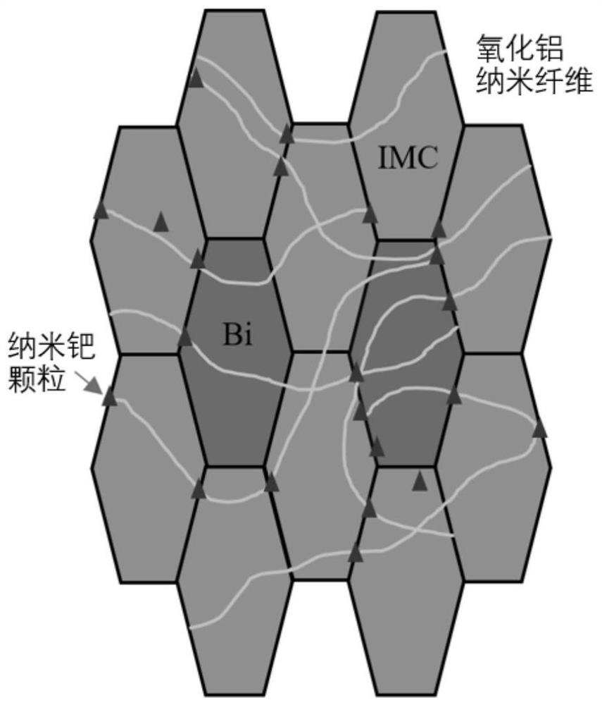
[0020] The composition and mass percentage of the Sn-based solder of the present invention are as follows: the content of aluminum oxide nanofibers is 1.0%, the content of nano-palladium particles is 3.0%, the content of Bi is 56%, and the balance is Sn.

[0021] Solder temperature performance test: under the premise of considering the experimental error, the solidus temperature is about 138.4 ℃, and the liquidus temperature is about 140.3 ℃.

Embodiment 2

[0023] The composition and mass percentage of the Sn-based solder of the present invention are as follows: the content of aluminum oxide nanofibers is 1.1%, the content of nano-palladium particles is 3.3%, the content of Bi is 56%, and the balance is Sn.

[0024] Solder temperature performance test: under the premise of considering the experimental error, the solidus temperature is about 138.5 ℃, and the liquidus temperature is about 140.6 ℃.

Embodiment 3

[0026] The composition and mass percentage of the Sn-based solder of the present invention are as follows: the content of aluminum oxide nanofibers is 1.2%, the content of nano-palladium particles is 3.6%, the content of Bi is 56%, and the balance is Sn.

[0027] Solder temperature performance test: under the premise of considering the experimental error, the solidus temperature is about 138.7 ℃, and the liquidus temperature is about 140.9 ℃.


PUM


Abstract

The invention discloses Sn-based brazing filler metal capable of achieving vertical stacking of chips and a bonding method of the Sn-based brazing filler metal. The Sn-based brazing filler metal comprises aluminum oxide nanofibers, nano palladium particles, Bi and Sn. The coupling effect of the aluminum oxide nanofibers, the nano palladium particles, Bi and Sn is utilized for strengthening welding spots, Bi-rich and IMC crystal grains can be tightly wound together by adding the aluminum oxide nanofibers, the nano palladium particles can be gathered at the grain boundaries of the Bi-rich and IMC crystal grains, the effect of pinning the aluminum oxide nanofibers and the grain boundaries is achieved, the aluminum oxide nanofibers and the nano palladium particles are coupled to reinforce the welding spots, so that the welding spots still keep higher strength and longer service life during the service period; the Sn-based brazing filler metal has good wettability and higher welding spot mechanical property, can meet the high reliability requirement of vertical stacking of high-density packaging and three-dimensional packaging electronic device chips, and can be used for wave soldering, reflow soldering and other brazing methods.

Description

technical field [0001] The invention relates to a Sn-based solder and a bonding method thereof, in particular to a Sn-based solder capable of realizing vertical stacking of chips and a bonding method thereof, and belongs to the technical field of chip-level packaging. Background technique [0002] With the development of Moore's Law, the miniaturization and multifunctionalization of electronic devices have become the engine for the development of the integrated circuit industry. The vertical stacking and interconnection of chips in three-dimensional space has successfully promoted the development of electronic products in the direction of miniaturization, integration and multi-function. Stacking technology is mainly used in various hardware, including 3D stacked memory, graphics processing unit (GPU), field programmable gate array (FPGA) and CMOS image sensor (CIS). According to the research report of the research institution YOLE, by 2023, The total value of the chip stack...

Claims


Application Information

Patent Timeline
IPC IPC(8): H01L23/488H01L21/60B23K35/26B82Y40/00B82Y30/00
CPCH01L24/13H01L24/11H01L24/82H01L24/81B23K35/264B82Y30/00B82Y40/00H01L2224/13113H01L2224/13164H01L2224/13111H01L2224/13187H01L2224/81801H01L2224/82801
Inventor 张亮李志豪郭永环何鹏李木兰
Owner XUZHOU NORMAL UNIVERSITY
Why Eureka
Try Eureka