A method of mixing rare earth materials in the growth of two -dimensional materials CVD

A technology of rare earth materials and two-dimensional materials, applied in the field of two-dimensional materials, can solve the problems of long photoelectric response time, low quantum efficiency and carrier mobility of two-dimensional materials, and limited applications, and achieves the improvement of photoelectric response performance. The effect of improving electrical and optoelectronic properties, photoresponse spectral width

Active Publication Date: 2022-08-09
CHONGQING INST OF GREEN & INTELLIGENT TECH CHINESE ACADEMY OF SCI +1
View PDF5 Cites 0 Cited by
  • Summary
  • Abstract
  • Description
  • Claims
  • Application Information

AI Technical Summary

Problems solved by technology

[0004] However, since a large number of atomic defects are inevitably generated during the growth of two-dimensional materials, and the volume of two-dimensional materials is the surface, these surface defects have a more serious impact on the photoelectric properties of two-dimensional materials, resulting in transition metals The quantum efficiency and carrier mobility of chalcogenide two-dimensional materials are low, and the photoelectric response time is generally long (ms level), etc., which limit their application in high-speed detection.
[0005] Therefore, it is an urgent problem for those skilled in the art to provide a method for doping rare earth materials in the CVD growth of two-dimensional materials to solve the application limitations of transition metal chalcogenide two-dimensional materials.

Method used


Image

  • A method of mixing rare earth materials in the growth of two -dimensional materials CVD
  • A method of mixing rare earth materials in the growth of two -dimensional materials CVD
  • A method of mixing rare earth materials in the growth of two -dimensional materials CVD

Examples


Embodiment 1

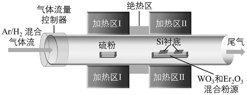
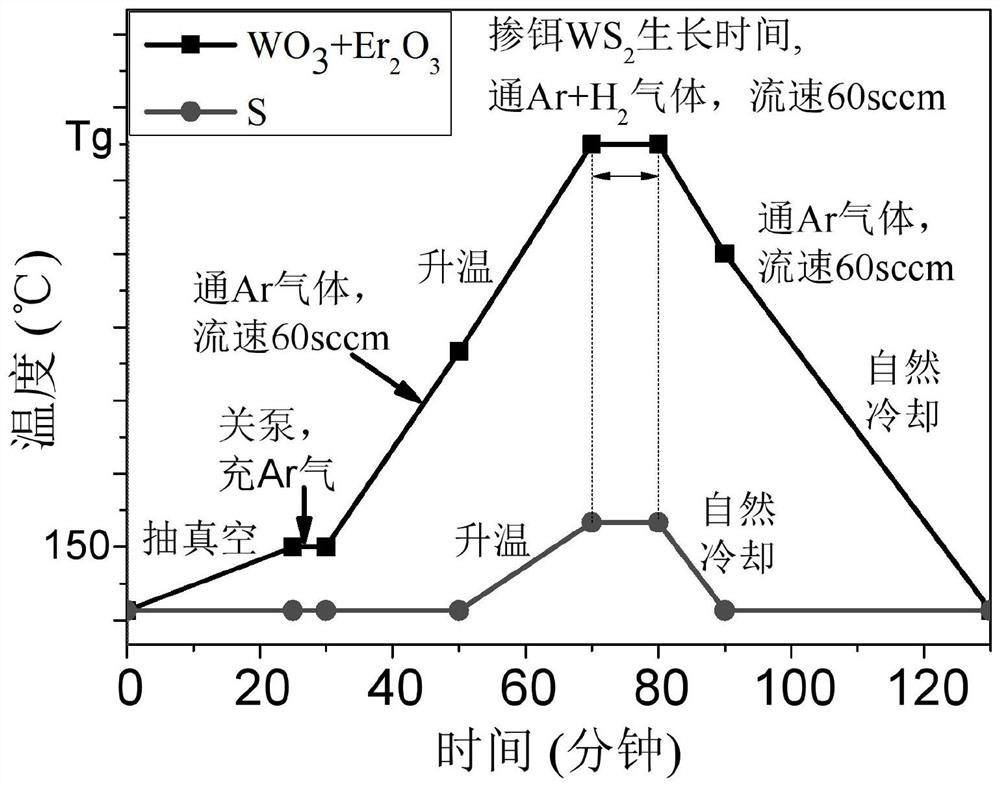
[0052] Embodiment 1 of the present invention provides a method for doping rare earth materials in the CVD growth of two-dimensional materials. The experiment of doped tungsten disulfide two-dimensional material is carried out in a dual-temperature zone vacuum tube furnace. The experimental device is as follows: figure 1 As shown, the grown erbium-doped tungsten disulfide WS 2 The schematic diagram of the temperature and airflow settings during the (Er) 2D material process is shown in Fig. figure 2 shown.

[0053] Specifically include the following steps:

[0054] (1) The substrate selected for the preparation of the sample is a single crystal silicon wafer with surface polishing or a single crystal silicon wafer with surface polishing and oxidation; before preparing the sample, the substrate needs to be cleaned to remove surface impurities; the substrate is immersed in acetone, alcohol, Ultrasonic cleaning was performed in deionized water for 10 min respectively; then the c...

Embodiment 2

[0064] The technical solution disclosed in Example 2 of the present invention is basically the same as that in Example 1, except that the sulfur powder is replaced with selenium powder, which is used to prepare tungsten selenide.


PUM


Abstract

The invention discloses a method for doping rare earth materials in the CVD growth of two-dimensional materials. The purpose of improving the performance of two-dimensional materials is achieved by doping rare earth elements in the process of growing two-dimensional materials. Specifically, it includes three main stages: the first stage is to prepare materials; the second stage is to place three powder sources, set the distance between the three powder sources, set the substrate material and WO 3 and Er 2 O 3 Vertical height between mixed powder sources; Erbium-doped WS grown using chemical vapor deposition in the third stage 2 (Er) two-dimensional material, in this stage, the heating rate of the three powder sources and the holding temperature of the three powder sources during the chemical reaction are set, and the gas flow rate is set.

Description

technical field [0001] The invention relates to the technical field of two-dimensional materials, and more particularly to a method for doping rare earth materials in the CVD growth of two-dimensional materials. Background technique [0002] In 2010, the Nobel Prize in Physics was awarded to Novoselov and Geim for the successful isolation of graphene, the first two-dimensional material with a thickness of a single atom in human history. Graphene has excellent mechanical, thermal, electrical and optical properties, which can play a powerful role in solar cells, supercapacitors, photodetectors, biological devices, gas sensors and other fields, and has broad application prospects. However, single-layer graphene is a gapless Dirac semimetal, which limits its application in electronic, optoelectronic and optical devices. [0003] In the process of graphene research, scientific researchers gradually expanded their horizons to other materials with similar structures to graphene, s...

Claims


Application Information

Patent Timeline
Patent Type & Authority Patents(China)
IPC IPC(8): C30B29/46C30B25/02C30B25/16C30B25/14
CPCC30B29/46C30B25/02C30B25/16C30B25/14Y02E10/549
Inventor 王春香赵洪泉石轩张国欣张炜
Owner CHONGQING INST OF GREEN & INTELLIGENT TECH CHINESE ACADEMY OF SCI
Why Eureka
Try Eureka