Electrooptical sensor static bias point process correction method and electro-optical sensor

An electro-optic sensor and static bias technology, applied in the field of sensors, can solve the problems of reducing the anti-electromagnetic interference performance of electro-optic sensors, failing to realize the π/2 static bias point, increasing the interference of electro-optic sensors, etc., and achieving good size reduction characteristics and structure Simple, effective method

Pending Publication Date: 2022-05-10
TSINGHUA UNIV
0 Cites 0 Cited by

AI-Extracted Technical Summary

Problems solved by technology

This method is costly, low yield, time-consuming and labor-intensive, and cannot achieve an accurate π/2 static bias point, which affects the accuracy of electric field measurement
[0006] In addition, there are technologies to modulate the static bias point of the electro-optic sensor through active monitoring and feedback control methods. Not only is the electro-optic sensor system compl...

Method used

By adjusting the dielectric constant of the transition group metal oxide resistive material, the static bias point of the electro-optic sensor is accurately reached to π/2 after the completion of the production, and the unavoidable process error is corrected in the production of the electro-optic sensor, and the electro-optic sensor is improved. The yield rate of the sensor chip and the method are efficient, which reduces the production cost of the electro-optical sensor; the external voltage used to adjust the dielectric constant of the transition metal oxide resistive material will be removed after the adjustment is completed, and the transition metal oxide resistive material The dielectric constant remains unchanged, so the effective refractive index of the optical waveguide remains uncha...

Abstract

The invention discloses an electro-optical sensor static bias point process correction method and an electro-optical sensor, and the electro-optical sensor static bias point process correction method comprises the following steps: measuring the deviation between the static bias point of the electro-optical sensor and pi/2; and the effective refractive index of the optical waveguide is adjusted, so that the static bias point of the electro-optical sensor reaches pi/2. External voltage is applied to the two sides of the transition metal oxide resistive material to adjust the dielectric constant of the transition metal oxide resistive material, so that the effective refractive index of the optical waveguide is changed, the static bias point reaches pi/2, and difficult-to-avoid process errors in manufacturing of the electro-optical sensor are corrected; the external voltage can be removed after the adjustment is completed, and the dielectric constant of the transition metal oxide resistive material is not changed, so that the effective refractive index of the optical waveguide is not changed, and the technology is passive; the transition metal oxide resistive material has a continuous light adjusting function, and the dielectric constant is continuously changed under excitation of different voltages, so that different application requirements are met.

Application Domain

Technology Topic

Image

  • Electrooptical sensor static bias point process correction method and electro-optical sensor
  • Electrooptical sensor static bias point process correction method and electro-optical sensor
  • Electrooptical sensor static bias point process correction method and electro-optical sensor

Examples

  • Experimental program(4)

Example Embodiment

[0079] Example 1:
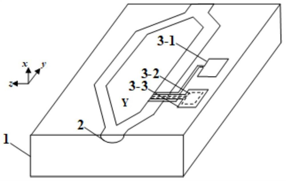
[0080] like figure 1 As shown, the substrate 1 of the electro-optic sensor is a bulk lithium niobate substrate, so the electro-optic sensor does not include the bonding buffer layer 4 and the support material 5 . Lithium niobate optical waveguide 2 adopts MZ interference optical path made by titanium diffusion or proton exchange process. The lower electrode 3-1 is made of indium tin oxide (ITO); the transition metal oxide resistive material layer 3-2 is made of tungsten trioxide (WO 3 ); the upper electrode 3-3 is made of indium tin oxide. Wherein, both Y branches in the MZ interference optical path can be replaced by a multimode interferometer (MMI).
[0081] In this technical solution, the tangential direction of the bulk lithium niobate substrate is x-cut, and the propagation direction of light is along the y-direction. The crystal coordinate system is as figure 1 The middle axis is shown.

Example Embodiment

[0082] Example 2:
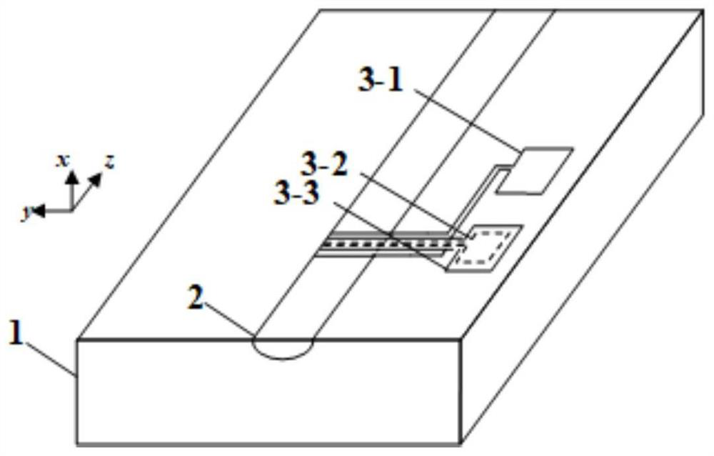
[0083] like figure 2 As shown, the substrate 1 of the electro-optic sensor is a bulk lithium niobate substrate, so the electro-optic sensor does not include the bonding buffer layer 4 and the support material 5 . The lithium niobate optical waveguide 2 is a common path interference optical path made by titanium diffusion or proton exchange technology. The lower electrode 3-1 is made of fluorine-doped tin oxide (FTO); the transition metal oxide resistive material layer 3-2 is made of titanium dioxide (TiO 2 ); the upper electrode 3-3 uses platinum (Pt).
[0084] In this technical solution, the tangent direction of the bulk lithium niobate substrate is x-cut, and the propagation direction of light is along the z-direction. The crystal coordinate system is as figure 2 The middle axis is shown.

Example Embodiment

[0085] Example 3:
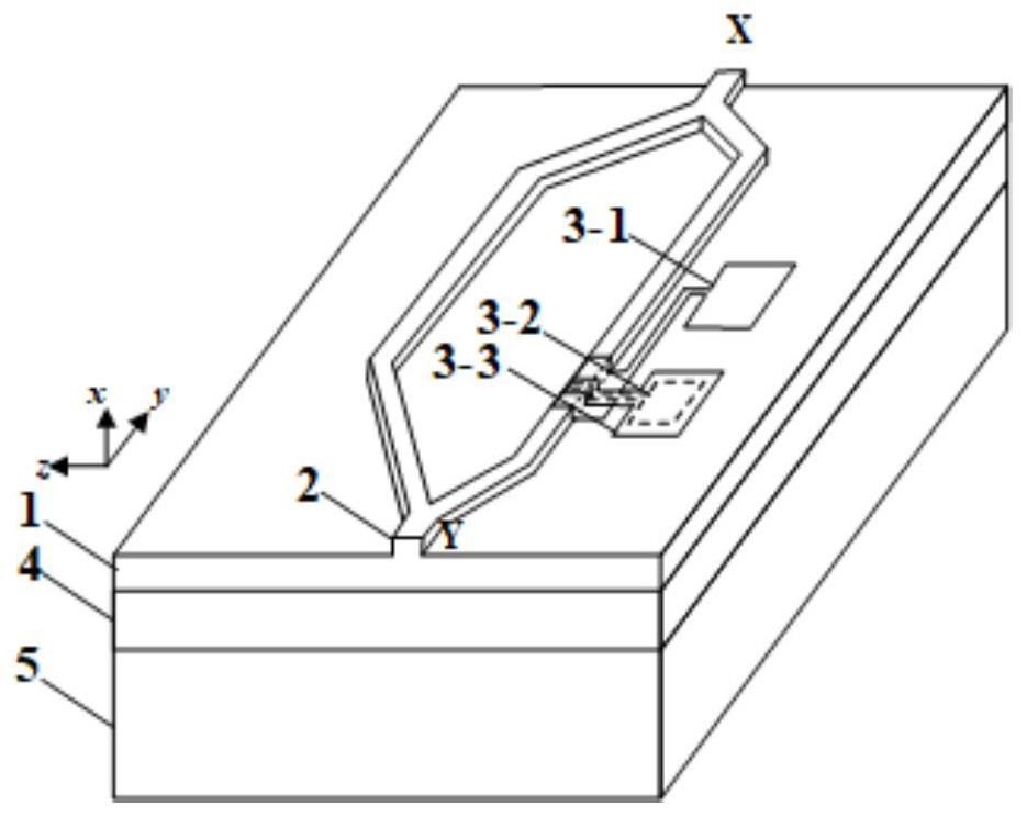
[0086] like image 3 As shown, the substrate 1 of the electro-optical sensor uses thin-film lithium niobate, which needs to be placed on the surface of the support material 5 through the bonding buffer layer 4 . Lithium niobate optical waveguide 2 is an MZ interference optical path made by etching or laser processing technology. The lower electrode 3-1 is made of indium tin oxide (ITO); the transition metal oxide resistive material layer 3-2 is made of niobium pentoxide (Nb 2 o 5 ); the upper electrode 3-3 is made of fluorine-doped tin oxide. The bonding buffer layer 4 is made of silicon dioxide. The support material 5 is block lithium niobate.
[0087] In this technical solution, the tangent direction of the lithium niobate film is x-cut, and the propagation direction of light is along the y direction. The crystal coordinate system is as image 3 The middle axis is shown.

PUM

no PUM

Description & Claims & Application Information

We can also present the details of the Description, Claims and Application information to help users get a comprehensive understanding of the technical details of the patent, such as background art, summary of invention, brief description of drawings, description of embodiments, and other original content. On the other hand, users can also determine the specific scope of protection of the technology through the list of claims; as well as understand the changes in the life cycle of the technology with the presentation of the patent timeline. Login to view more.

Similar technology patents

Thick plate rolling method

ActiveCN102886381AImprove the plane shape of the steel plateImprove yieldMetal rolling arrangementsProfile control deviceSteel platesShape control
Owner:BAOSHAN IRON & STEEL CO LTD

Classification and recommendation of technical efficacy words

  • Efficient method
  • Improve yield

Krill oil process

Owner:PRONOVA BIOPHARMA NORGE

Method for preparing porous alumina ceramic supporting body with sol as additive

InactiveCN101412620ASolve the cracking problemImprove yieldHoneycombAlumina ceramic
Owner:XI AN JIAOTONG UNIV
Why Eureka
Try Eureka