Annealed Si-based InN nanorod heterojunction and preparation method and application thereof

An annealing treatment and nano-pillar technology is applied in the field of InN nano-pillars to achieve the effects of saving preparation cost, reducing migration distance and reducing recombination probability

Pending Publication Date: 2022-06-24
SOUTH CHINA UNIV OF TECH
View PDF7 Cites 3 Cited by
  • Summary
  • Abstract
  • Description
  • Claims
  • Application Information

AI Technical Summary

Problems solved by technology

[0003] Chemical vapor deposition is a material preparation method with low cost and simple process, but there is no literature that discloses the method of preparing InN nanopillars in different atmospheres (N 2 Protected sulfur atmosphere, oxygen atmosphere and selenium atmosphere) annealing to prepare InN nanopillar heterojunctions, so as to realize high-efficiency photoelectrochemical water splitting photoelectrode based on InN nanopillars

Method used


Image

  • Annealed Si-based InN nanorod heterojunction and preparation method and application thereof
  • Annealed Si-based InN nanorod heterojunction and preparation method and application thereof
  • Annealed Si-based InN nanorod heterojunction and preparation method and application thereof

Examples


Embodiment 1

[0037] A preparation method of an annealed Si-based InN nano-pillar heterojunction, comprising the following steps:

[0038] (1) Substrate selection: n-type Si substrate (conductivity <0.005Ω) is used.

[0039] (2) Growth of InN nanocolumns: the molecular beam epitaxy growth process is used, the substrate temperature in step (1) is controlled to be 400 °C, the substrate rotation speed is 10 r / min, and the In beam equivalent pressure is 1.43×10 -7 Torr, the nitrogen flow rate was 2sccm, the plasma source power was 400W, and the growth time was 2h.

[0040] (3) Preparation method of InN nano-pillar heterojunction: chemical vapor deposition process is used to deposit the prepared InN nano-pillars in N 2 Annealed at 500 °C for 5 min in a protected sulfur atmosphere to obtain InN / In 2 S 3 Nanopillar heterojunction.

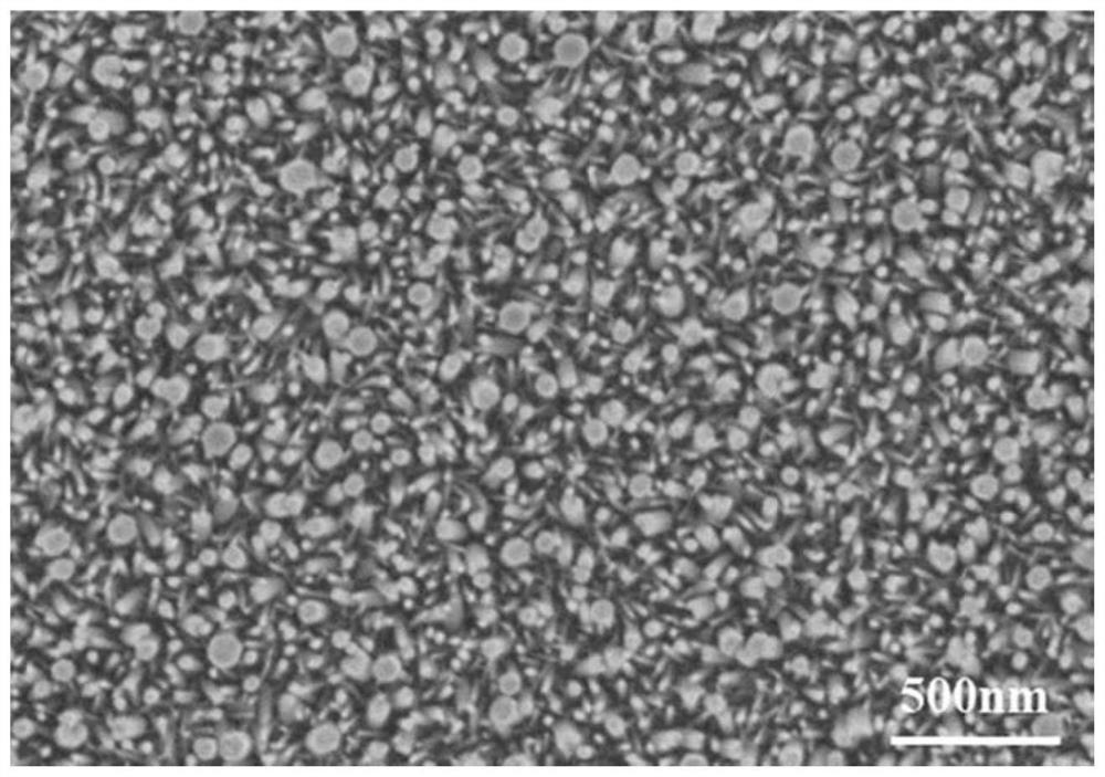
[0041] like figure 1 As shown, the SEM top view of the Si-based InN nano-pillar heterojunction annealed in a sulfur atmosphere in this example.
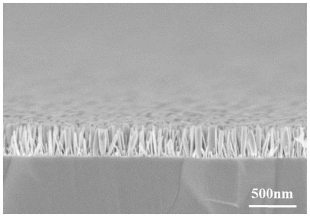
[0042] like f...

Embodiment 2

[0045] A preparation method of an annealed Si-based InN nano-pillar heterojunction, comprising the following steps:

[0046] (1) Substrate selection: n-type Si substrate (conductivity <0.005Ω) is used.

[0047] (2) Growth of InN nanocolumns: the molecular beam epitaxy growth process is used, the substrate temperature in step (1) is controlled to be 400 °C, the substrate rotation speed is 10 r / min, and the In beam equivalent pressure is 1.43×10 -7 Torr, the nitrogen flow rate was 2sccm, the plasma source power was 400W, and the growth time was 2h.

[0048] (3) Preparation method of InN nano-pillar heterojunction: chemical vapor deposition process is used to deposit the prepared InN nano-pillars in N 2 Annealed at 500 °C for 5 min in an oxygen atmosphere under protection to obtain InN / In 2 O 3 Nanopillar heterojunction.

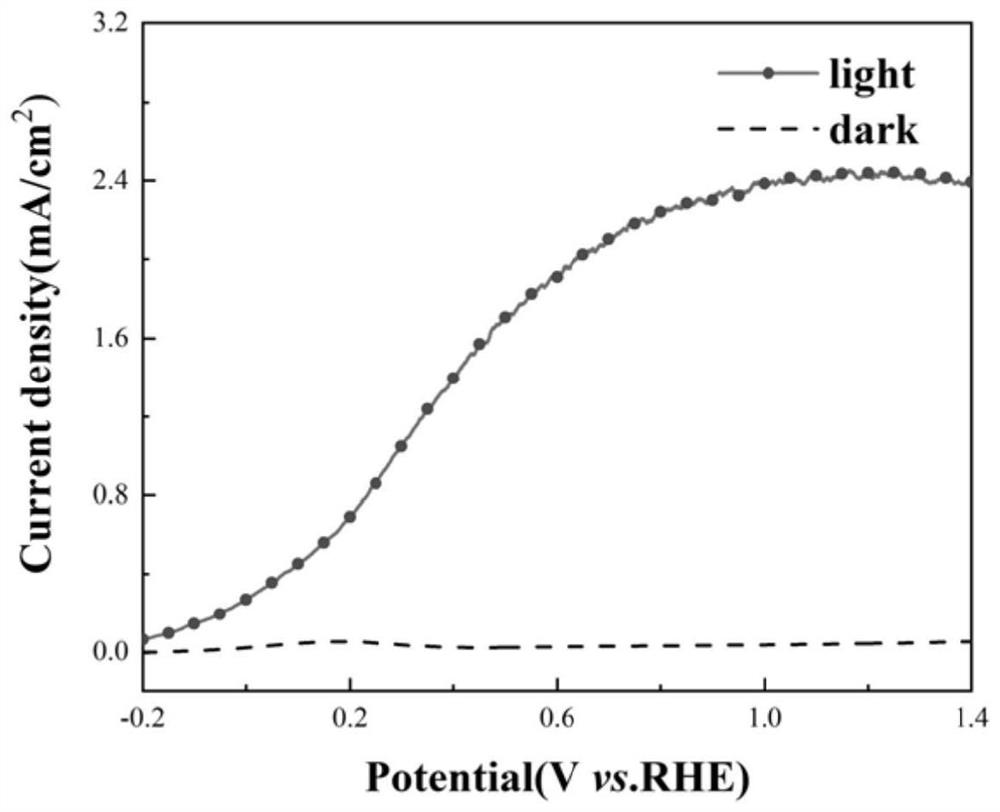
[0049]The Si-based InN nanopillar heterojunction annealed in the sulfur atmosphere of this example is used for photoelectrolysis of water: the prepared Si-...

Embodiment 3

[0051] A preparation method of an annealed Si-based InN nano-pillar heterojunction, comprising the following steps:

[0052] (1) Substrate selection: n-type Si substrate (conductivity <0.005Ω) is used.

[0053] (2) Growth of InN nanopillars: using the molecular beam epitaxy growth process, the substrate temperature in step (1) is controlled to be 400 °C, the substrate rotation speed is 10 r / min, and the In beam equivalent pressure is 1.43×10 -7 Torr, the nitrogen flow rate was 2sccm, the plasma source power was 400W, and the growth time was 2h.

[0054] (3) Preparation method of InN nano-pillar heterojunction: chemical vapor deposition process is used to deposit the prepared InN nano-pillars in N 2 Annealed at 500 °C for 5 min in a protected selenium atmosphere to obtain InN / In 2 Se 3 Nanopillar heterojunction.

[0055] The Si-based InN nanopillar heterojunction annealed in the sulfur atmosphere of this example is used for photoelectrolysis of water: the prepared Si-based ...


PUM

PropertyMeasurementUnit
heightaaaaaaaaaa
diameteraaaaaaaaaa

Abstract

The invention discloses an annealed Si-based InN nanorod heterojunction as well as a preparation method and application of the annealed Si-based InN nanorod heterojunction. The preparation method comprises the following steps: (1) growing an InN nanorod on a Si substrate by adopting a molecular beam epitaxial growth process; (2) carrying out annealing treatment on the InN nanorod obtained in the step (1) to obtain a Si-based InN nanorod heterojunction; the annealing atmosphere is a sulfur atmosphere, an oxygen atmosphere or a selenium atmosphere under the protection of N2. The InN nanorod heterojunction comprises a substrate and an InN nanorod grown on the substrate, wherein the InN nanorod is annealed in different atmospheres to form the heterojunction. The Si-based InN nanorod heterojunction photoelectrode is prepared by adopting a method which is low in cost and simple in process. The heterojunction photoelectrode can be used for hydrogen production through photoelectrocatalysis water decomposition, the hydrogen production efficiency is greatly improved, and an effective strategy is provided for large-scale preparation of hydrogen energy through solar energy.

Description

technical field [0001] The invention relates to the field of InN nano-pillars, in particular to an annealed Si-based InN nano-pillar heterojunction and a preparation method and application thereof. Background technique [0002] Photoelectrochemical water splitting for hydrogen production shows great potential in solving the global energy crisis and environmental problems. InN nanopillars have a small band gap (0.65 eV), a suitable band position for water oxidation, and thus become an option for photoanode. In addition, InN nanopillars possess a suitable energy band position for water redox reaction and high surface area to volume ratio, making InN nanopillars promising for efficient photoelectrochemical water splitting. However, the fast recombination of bulk and surface charges and slow oxidation reaction kinetics of InN nanopillars lead to the need for additional bias to facilitate charge transfer. Today, building semiconductor heterostructures to tune the energy bands o...

Claims


Application Information

Patent Timeline
Patent Type & Authority Applications(China)
IPC IPC(8): C30B29/40C30B33/02C30B25/02C25B11/052C25B11/059C25B11/087C25B1/04C25B1/55B82Y40/00
CPCC30B29/403C30B33/02C30B25/02C25B11/052C25B11/059C25B11/087C25B1/04C25B1/55B82Y40/00
Inventor 李国强刘乾湖谢少华梁杰辉
Owner SOUTH CHINA UNIV OF TECH
Why Eureka
Try Eureka