D15-mode ferroelectric single crystal film piezoelectric vibration sensor and preparation method thereof
A ferroelectric single crystal, piezoelectric vibration technology, applied in piezoelectric/electrostrictive/magnetostrictive devices, circuits, electrical components, etc., can solve problems affecting voltage output, corresponding sensitivity and device performance, and achieve improved Effect of voltage output and sensitivity, low performance drop in low temperature environment, and high electromechanical conversion efficiency
- Summary
- Abstract
- Description
- Claims
- Application Information
AI Technical Summary
Problems solved by technology
Method used
Image

Examples
preparation example Construction
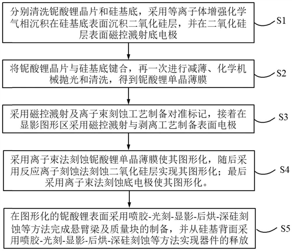
[0028] The embodiments of the present application provide a d 15 The preparation method of the mode ferroelectric single crystal thin film piezoelectric vibration sensor comprises the following steps:
[0029] S1: respectively cleaning the lithium niobate wafer and the silicon substrate, depositing a silicon dioxide layer on the surface of the silicon substrate by plasma enhanced chemical vapor deposition, and magnetron sputtering the bottom electrode on the surface of the silicon dioxide layer;
[0030] S2: bonding the lithium niobate wafer with the silicon substrate, and then performing thinning, chemical mechanical polishing and cleaning in sequence to obtain a lithium niobate single crystal thin film;
[0031] S3: use magnetron sputtering and ion beam etching processes to prepare alignment marks, and then use magnetron sputtering and stripping processes to prepare surface electrodes in the developing pattern area;
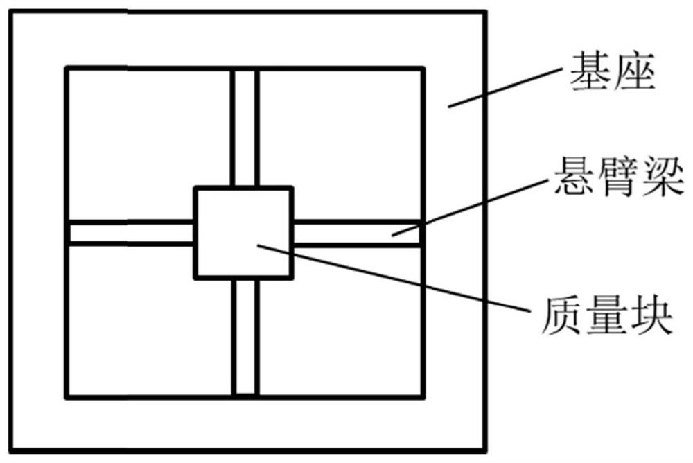
[0032] S4: The lithium niobate single crystal thin film ...
Embodiment 1
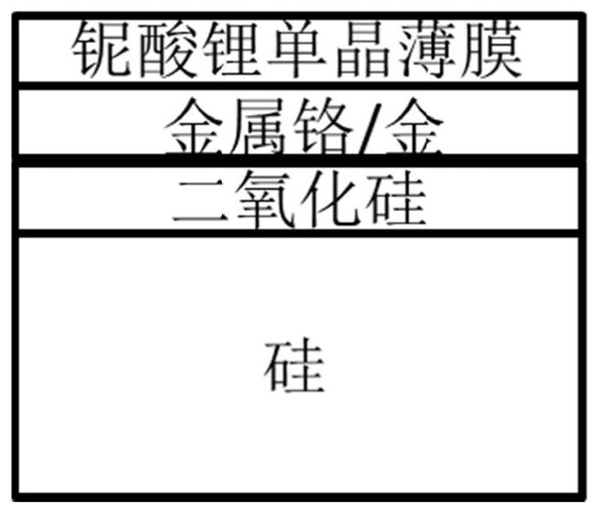
[0052] Step 1. Prepare a lithium niobate single crystal thin film with a bottom electrode / silicon dioxide layer / silicon as the base. The specific method is as follows:
[0053] a. The lithium niobate wafer and the silicon substrate are respectively ultrasonicated with acetone, isoacetone, absolute ethanol and deionized water for 5 minutes respectively, rinsed with deionized water, and dried with nitrogen to remove organic matter and impurities on the surface;
[0054] b using plasma enhanced chemical vapor deposition to grow a 2μm silicon dioxide layer on a silicon substrate;
[0055] c Magnetron sputtering bottom electrode on the surface of the silicon dioxide layer, the power of the magnetron sputtering equipment is 500W, 20nm metal chromium is sputtered on the surface of the silicon dioxide layer as the adhesion layer, and 200nm gold is used as the bottom electrode to obtain a The process side of the direct bonding process;
[0056] d Repeat step (a) to clean the silicon s...
Embodiment 2
[0078] Step 1. Prepare a lithium niobate single crystal thin film with a bottom electrode / silicon dioxide layer / silicon as the base. The specific method is as follows:
[0079] a. The lithium niobate wafer and the silicon substrate are respectively ultrasonicated with acetone, isoacetone, absolute ethanol and deionized water for 5 minutes respectively, rinsed with deionized water, and dried with nitrogen to remove organic matter and impurities on the surface;
[0080] b using plasma enhanced chemical vapor deposition to grow a 1μm silicon dioxide layer on a silicon substrate;
[0081] c Magnetron sputtering bottom electrode on the surface of the silicon dioxide layer, the power of the magnetron sputtering equipment is 400W, 10nm metal chromium is sputtered on the surface of the silicon dioxide layer as the adhesion layer, and 100nm gold is used as the electrode to obtain a direct The technological side of the bonding process;
[0082] d Repeat step (a) to clean the silicon subs...
PUM
| Property | Measurement | Unit |
|---|---|---|
| Thickness | aaaaa | aaaaa |
| Thickness | aaaaa | aaaaa |
| Thickness | aaaaa | aaaaa |
Abstract
Description
Claims
Application Information
 - R&D
- Intellectual Property
- Life Sciences
- Materials
- Tech Scout
- Unparalleled Data Quality
- Higher Quality Content
- 60% Fewer Hallucinations
Browse by: Latest US Patents, China's latest patents, Technical Efficacy Thesaurus, Application Domain, Technology Topic, Popular Technical Reports.
© 2025 PatSnap. All rights reserved.Legal|Privacy policy|Modern Slavery Act Transparency Statement|Sitemap|About US| Contact US: help@patsnap.com