LED epitaxial wafer manufacturing method

A technology of LED epitaxial wafers and manufacturing methods, which is applied in the direction of semiconductor devices, electrical components, circuits, etc., can solve the problems of affecting LED energy saving effect, hindering LED performance, and low LED performance, so as to reduce material growth defects and improve internal quantum efficiency , Improve the effect of crystal quality

Pending Publication Date: 2022-07-29
XIANGNENG HUALEI OPTOELECTRONICS
View PDF0 Cites 1 Cited by
  • Summary
  • Abstract
  • Description
  • Claims
  • Application Information

AI Technical Summary

Problems solved by technology

At present, the scale of domestic production of LEDs is gradually expanding, but LEDs still have the problem of low performance, which affects the energy-saving effect of LEDs
[0003] At present, the quantum efficiency of LED epitaxial multi-quantum wells prepared by the existing LED epitaxial wafer method is not high, which seriously hinders the improvement of LED performance and affects the energy-saving effect of LED.
[0004] In summary, there is an urgent need to develop new LED epitaxial wafer manufacturing methods, improve the crystal quality of quantum wells, and solve the problem of low quantum efficiency in existing LED multi-quantum wells, thereby improving the luminous efficiency of LEDs

Method used


Image

  • LED epitaxial wafer manufacturing method
  • LED epitaxial wafer manufacturing method
  • LED epitaxial wafer manufacturing method

Examples


Embodiment 1

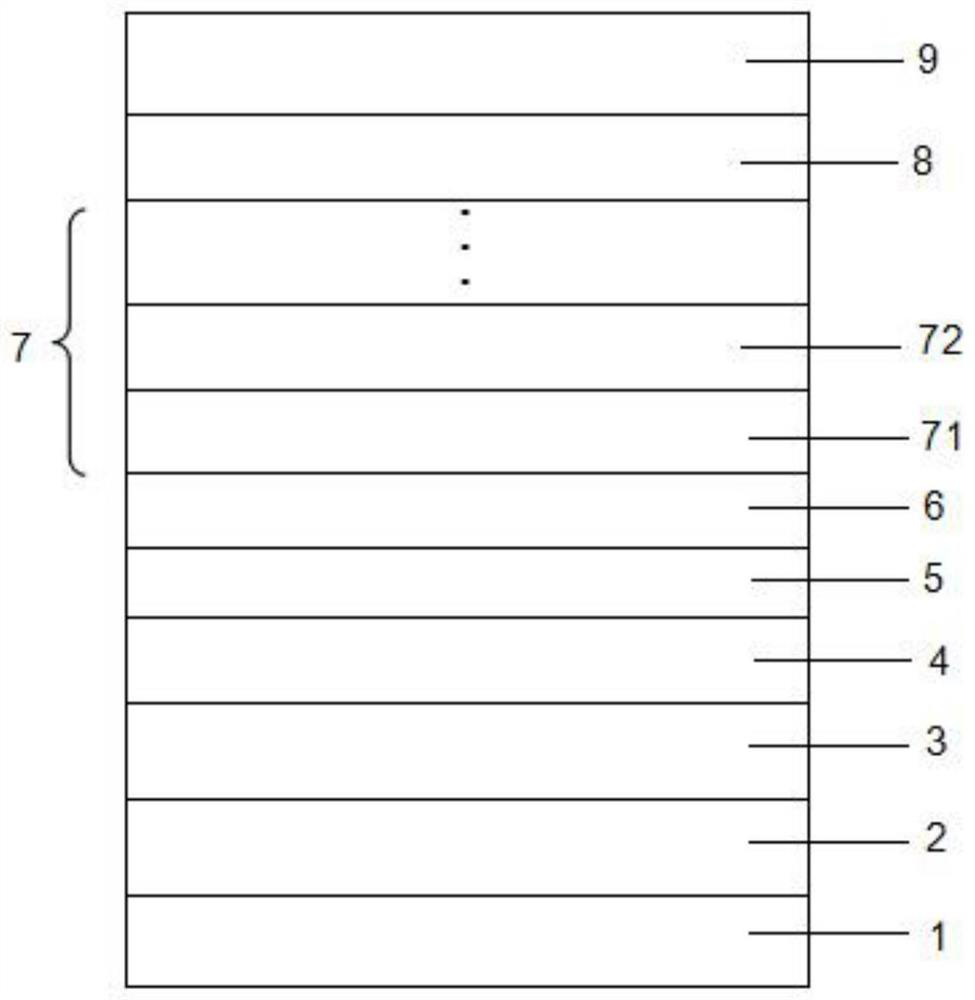
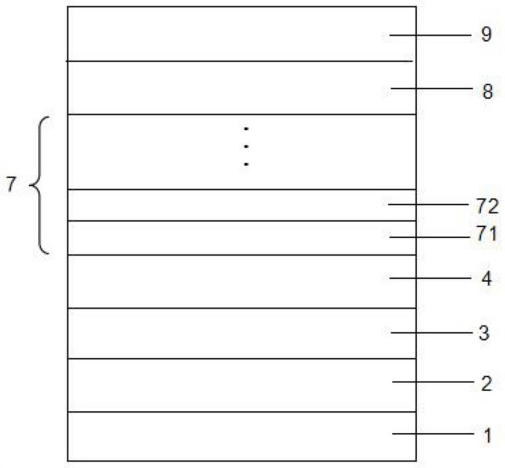
[0037] This embodiment adopts the LED epitaxial wafer fabrication method provided by the present invention, adopts MOCVD to grow GaN-based LED epitaxial wafers, and adopts high-purity H 2 or high purity N 2 or high purity H 2 and high purity N 2 Mixed gas as carrier gas, high purity NH 3 As N source, metal organic source trimethyl gallium (TMGa) as gallium source, trimethyl indium (TMIn) as indium source, and N-type dopant as silane (SiH 4 ), trimethylaluminum (TMAl) was used as the aluminum source, and the P-type dopant was magnesium dimethylocene (CP). 2 Mg), the reaction pressure was between 70 mbar and 600 mbar. The specific growth method is as follows (for the epitaxial structure, please refer to figure 1 ):

[0038] The LED epitaxial wafer fabrication method includes in sequence: processing a sapphire substrate 1, growing a low-temperature GaN buffer layer 2, growing an undoped GaN layer 3, growing a Si-doped n-type GaN layer 4, sputtering a molybdenum oxide layer ...


PUM

PropertyMeasurementUnit
thicknessaaaaaaaaaa
thicknessaaaaaaaaaa
thicknessaaaaaaaaaa

Abstract

The invention discloses a method for manufacturing an LED epitaxial wafer, and the method sequentially comprises the steps: processing a substrate, growing a low-temperature GaN buffer layer, growing a non-doped GaN layer, growing a Si-doped n-type GaN layer, manufacturing a carrier transition layer, growing a multi-quantum well layer, growing an AlGaN electron blocking layer, growing a Mg-doped P-type GaN layer, and carrying out the cooling. Wherein the step of manufacturing the carrier transition layer sequentially comprises the steps of sputtering a molybdenum oxide layer, performing ozone treatment and manufacturing a nitrogen atom layer. According to the invention, the crystal quality of the quantum well is improved by adopting the new manufacturing method, so that the luminous efficiency of the LED is improved.

Description

technical field [0001] The invention belongs to the technical field of semiconductors, and in particular relates to a manufacturing method of an LED epitaxial wafer. Background technique [0002] Light-Emitting Diode (LED) is a semiconductor electronic device that converts electrical energy into light energy. When a current flows through the LED, the electrons and holes in the LED recombine in its multiple quantum wells to emit monochromatic light. As a high-efficiency, environmentally friendly and green new solid-state lighting source, LED has the advantages of low voltage, low energy consumption, small size, light weight, long life, high reliability and rich colors. At present, the scale of domestic LED production is gradually expanding, but LED still has the problem of low performance, which affects the energy-saving effect of LED. [0003] At present, the LED epitaxial multiple quantum wells prepared by the existing LED epitaxial wafer method have low internal quantum ...

Claims


Application Information

Patent Timeline
Patent Type & Authority Applications(China)
IPC IPC(8): H01L33/00H01L33/12H01L33/06H01L33/14H01L33/32
CPCH01L33/0075H01L33/12H01L33/06H01L33/145H01L33/32
Inventor 徐平周孝维许孔祥
Owner XIANGNENG HUALEI OPTOELECTRONICS
Why Eureka
Try Eureka