Method for mfg. organic electroluminescent display panel covered with protective film

A manufacturing method and technology of protective film, applied in the direction of electroluminescence light source, electric light source, light source, etc., can solve the problems of long sealing process time, increase the cost of raw materials, shorten the life of accessories, etc., to overcome manufacturing difficulties, improve production efficiency, The effect of simplifying the process

Inactive Publication Date: 2003-10-29
朱星厚 +2
0 Cites 21 Cited by

AI-Extracted Technical Summary

Problems solved by technology

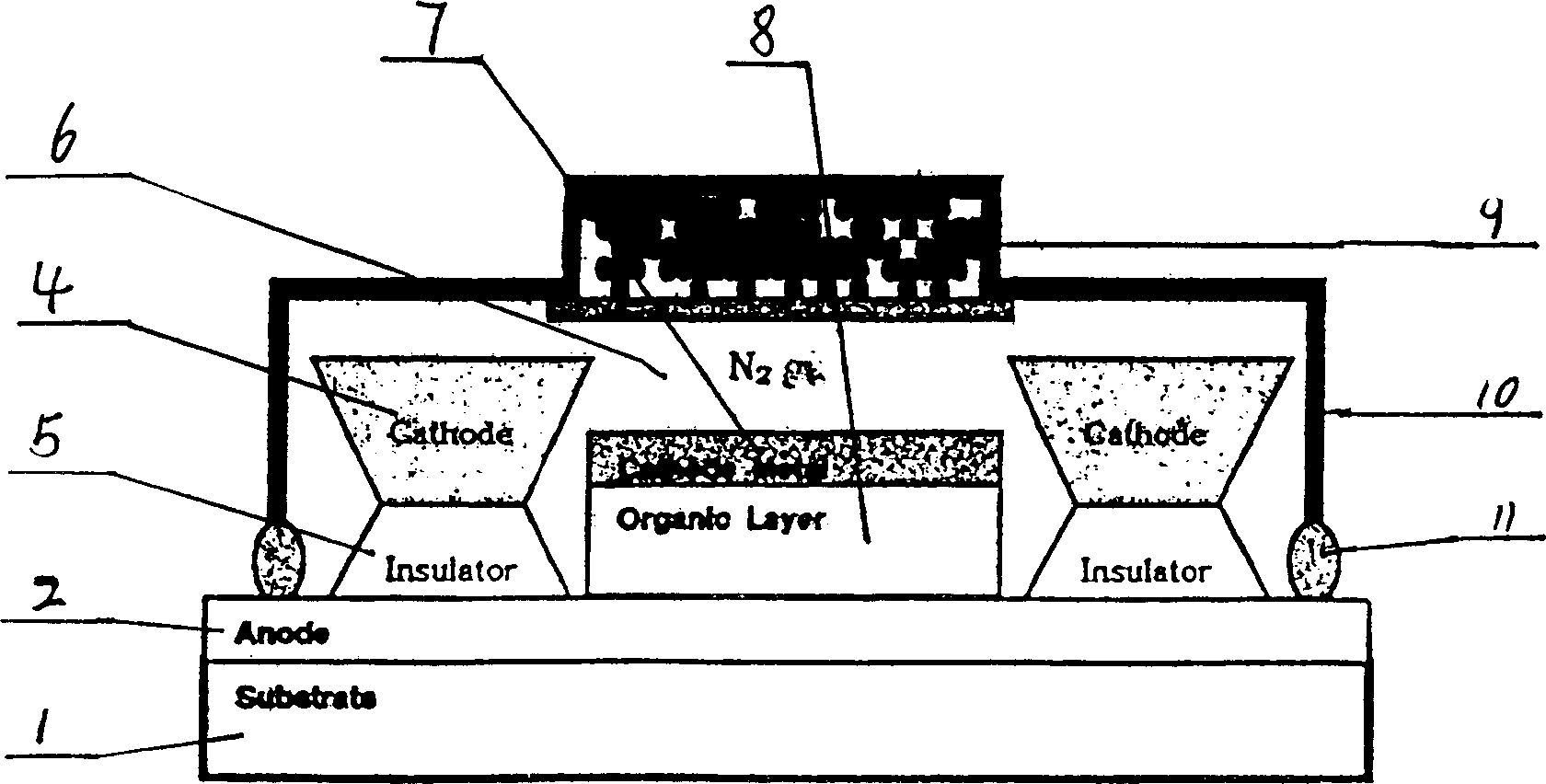
However, this pocket-type technology requires another layer (Metal Canister) or glass (Glass) on the substrate, which will have the following negative effects: (1) increase the thickness of the display panel; (2) paste the substrate The adhesive (Sealant) applied during the process with the metal cap (Capsule) may release some active gases, thereby shortening the life of the accessories; (3) components such as oxygen and moisture in the air can penetrate through the adhesive (Sealant) ), shorten the life of the accessories; (4) The application quality of the adhesive (Sealant) may cause the aging of the a...

Method used

(2) do not need prior art adhesive, hygroscopic agent, metal cover (Capsule) etc., and covered protective film, save production raw material cost;
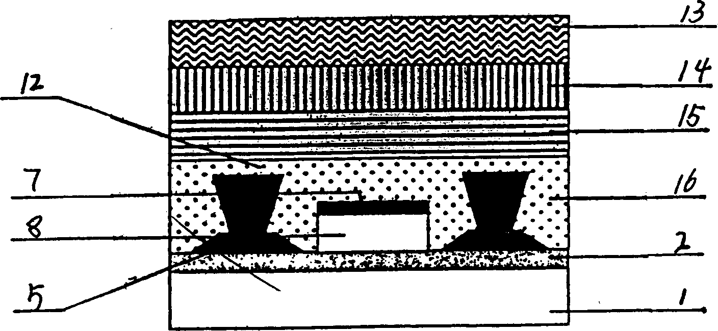
(3) after the organic film film-forming 16, manufacture can absorb the moisture that accessory produces or the hygroscopic layer 15 of oxygen, hygroscopic agent usually uses materials such as calcium oxide (CaO), barium oxide (BaO), zeolite (Zeolite), The film forming process adopts chemical vapor deposition (CVD), thermal evaporation (Thermal Evaporation), E-Beam Evaporation and other technical methods to reduce the impact on accessories.
[0018] (2) Use Alq3, Cupc and other raw materials to cover a layer of buffer organic film 16 above the substrate of the accessory to prevent the accessory from being damaged during the manufacturing process of the hygroscopic film and the protective film. The covering method of the buffer organic film 16 is the same as the covering method of the organic film 8 of the organic display panel assembly, and will not be repeated here.
[0021] (5) Then cover the upper part of the inorganic insulating film 14 with a certain thickness of high-strength polymer film 13 to prevent the penetration of...

Abstract

A process for preparing the organic electroluminescent display screen covered by protecting membranes is characterized by that the carrier substrate of the display screen is sequentially covered witha film able to absorb water and oxygen, an inorganic protecting film for preventing and stopping air, and a high-molecular film able to prevent penetration of external water and oxygen. Its advantages are thin thickness, low cost and high productivity.

Application Domain

Electrical apparatusElectroluminescent light sources

Technology Topic

ChemistryMolecular film +5

Image

  • Method for mfg. organic electroluminescent display panel covered with protective film
  • Method for mfg. organic electroluminescent display panel covered with protective film
  • Method for mfg. organic electroluminescent display panel covered with protective film

Examples

  • Experimental program(3)

Example Embodiment

[0023] Example 1:
[0024] like Figure 4 As shown, the manufacturing process of the parylene film: heating the dimer (Di-para-xylylene) under the pressure of 1.0 torr to 150 degrees Celsius , decomposed into monomer (Monomer) parylene, and then sprayed into the reaction chamber (Chamber) at a pressure of 0.5 torr not higher than 680 degrees Celsius, at a pressure of 25 degrees Celsius and 0.1 torr To form a polymer (Polymer) parylene (para-xylylene), that is, to form a film.

Example Embodiment

[0025] Example 2:
[0026] like Figure 5 As shown, silicone resin refers to an organic group-containing polymer (Polymer) connected by Si-O-Si bonding of silicon and oxygen. Therefore, it has both organic and inorganic properties. That is, by analyzing the molecular structure of silicone resin, due to the combination of Si-O-Si, it has inorganic properties such as heat resistance, chemical stability, abrasion resistance, and high gloss; at the same time, because of the organic properties of its side chains, it has Excellent reactivity, solubility, productivity, etc. According to the different forms of silicone resin, it is divided into oil (oil), rubber (Rubber), resin (Resin) and other types. The higher the degree of cross-linking of silicon (Silicon Resin), the lower the activity and flexibility of the molecule, and the higher the hardness. The product with extremely high crosslink density is Silicone Resin.

Example Embodiment

[0027] Example 3:
[0028] like Image 6 As shown, the chemical basic unit of epoxy resin must contain epoxy (Epoxy) structure, which is usually produced by neutralizing epichlorohydrin and bisphenol A. Epoxy resins are difficult to use alone and require the addition of a hardener. Therefore, epoxy resins in the strict sense are intermediate products. Because bisphenol A epoxide is produced by the reaction of 2,2-bis-p-hydroxyphenylpropane BPA (Bisphenol A) and chloromethoxy cyclopropane ECH (ie Epichlorohybrine), it belongs to the benzene ring nucleus (BisphenolA), so it is difficult to rotate freely . Therefore, its chemical resistance, adhesion, toughness, high temperature resistance and other properties are outstanding. In addition, the ether group in the molecule can improve chemical resistance and plasticity. Hydrophilic hydroxyl groups and hydrophobic hydrocarbon groups are regularly arranged, so its adhesion is excellent.

PUM

no PUM

Description & Claims & Application Information

We can also present the details of the Description, Claims and Application information to help users get a comprehensive understanding of the technical details of the patent, such as background art, summary of invention, brief description of drawings, description of embodiments, and other original content. On the other hand, users can also determine the specific scope of protection of the technology through the list of claims; as well as understand the changes in the life cycle of the technology with the presentation of the patent timeline. Login to view more.

Similar technology patents

Rotary damper

InactiveUS20050252740A1reduce thickness
Owner:SOMIC ISHIKAWA INC

Direct downward background module

InactiveCN1510482Areduce thickness
Owner:BENQ CORP

Thin film ink jet printhead adhesion enhancement

InactiveUS20050078151A1increase adhesionreduce thickness
Owner:FUNAI ELECTRIC CO LTD

Heat exchanger

Owner:DENSO CORP

Semiconductor package

Owner:ADVANCED SEMICON ENG INC

Classification and recommendation of technical efficacy words

  • overcome manufacturing difficulties
  • reduce thickness

Multi light source large view field spliced illumination system

ActiveCN104166312Aovercome manufacturing difficultiesOvercoming image plane inhomogeneity
Owner:SHANGHAI MICRO ELECTRONICS EQUIP (GRP) CO LTD
Why Eureka
Try Eureka