P type window layer in use for solar cell of silicon thin film, and preparation method

A solar cell and window layer technology, applied in circuits, photovoltaic power generation, electrical components, etc., can solve problems such as rarely seen P-type window layers, and achieve the effects of improving cell efficiency, high conductivity, and low cost

Active Publication Date: 2005-11-16
GS SOLAR FU JIAN COMPANY
View PDF0 Cites 12 Cited by
  • Summary
  • Abstract
  • Description
  • Claims
  • Application Information

AI Technical Summary

Problems solved by technology

So far, in the reports of microcrystalline silicon cells, we have rarely seen the preparation technology of P-type window layer that can satisfy the window characteristics at the same time without affecting the characteristics of the microcrystalline silicon active layer.

Method used


Image

  • P type window layer in use for solar cell of silicon thin film, and preparation method

Examples


preparation example Construction

[0014] The preparation method of p-type window layer for thin film solar cell, it comprises following 3 steps:

[0015] 1) Put the glass substrate G with T in the vacuum chamber, the background vacuum is lower than 10 -3 support;

[0016] 2) Plasma-enhanced chemical vapor deposition (PECVD) was used to deposit P 1 and P 2 Thin film, the glow excitation frequency used is: 13.56MHz-100MHz:

[0017] 3) The reaction gas introduced into the reaction chamber is: silane, hydrogen, borane or trimethyl boron, P 1 and P 2 Thin film reactive deposition parameters are as follows:

[0018] The reaction gas pressure is above 0.1 Torr (Torr);

[0019] Glow power density: 40 milliwatts (mW)-500 milliwatts (mW);

[0020] Substrate surface temperature: 100-260°C;

[0021] Hydrogen diluted silane concentration SC=([SiH 4 ] / ([SiH 4 ]+[H 2 ]))%≤5%;

[0022] Ratio of boron-containing gas to silane (boron dopant concentration): BS≤3%.

[0023] By adjusting the boron dopant concentration...

Embodiment 1

[0036] On Corning7059 glass substrate, adopt silane, hydrogen, borane as reaction source gas, by VHF-PECVD method, glow excitation frequency is 60MHz, according to the preparation method that this patent thin film solar cell uses p-type window layer included in The steps are to select the deposition process parameters and prepare the microcrystalline silicon p-layer material. Under the premise that the thickness is 20-30nm, its conductance can be at 10 -1 On the order of s / cm, the crystallization rate reaches 40%-50%.

Embodiment 2

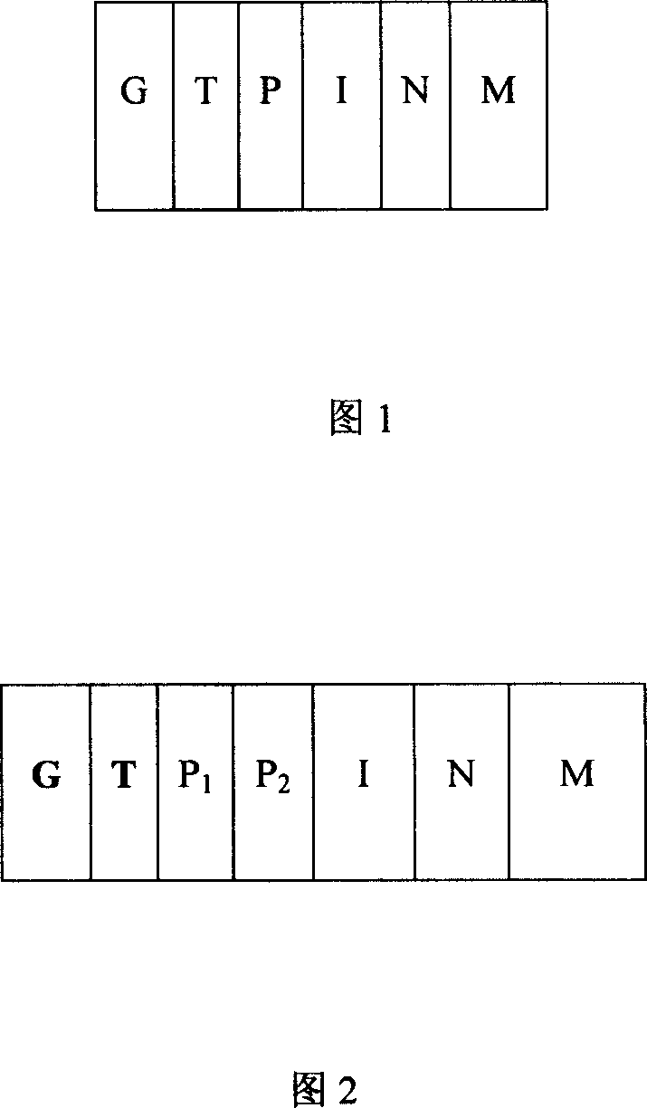
[0038] On the glass substrate covered with ZnO transparent conductive film, silane, hydrogen, borane and phosphine are used as reaction source gases, and the glow excitation frequency is 60MHz by VHF-PECVD method. According to the p-type thin film solar cell of this patent The steps included in the preparation method of the window layer select the deposition process parameters, and prepare the p-type window layer and the microcrystalline silicon thin film solar cell according to the steps shown in Figure 2 of the specification. When the cell area is 0.253 square centimeters, the efficiency of the prepared single-junction pin type microcrystalline silicon thin film solar cell reaches 9.2% (when carrying out J-V test, the used light intensity is AM1.5, 100mW / cm 2 ).


PUM


Abstract

The window layer is composed of transparent substrate, transparent conductive film and P type window layer etc. Characters are that P layer is divided into P1 and P2 layers. P1 layer is thin film of Nano silicon with high crystallizing rate and wide band gap. Thickness of P1 is smaller than thickness of P2 in one order of magnitude. Two-layered P type doping layer structure is adopted in designing P type window layer. Controlling crystallizing rates, doping concentrations and thickness in two layers reaches crystallizing and doping results to be completed respectively so as to meet requirement of high conductance and high crystallizing rate. The disclosed window layer provides good basis for further growth of active layer of crystallite silicon, raises battery efficiency by high open circuit voltage and low series resistance.

Description

technical field [0001] The invention relates to a window layer of a silicon-based thin-film solar cell, in particular to the structure and preparation technology of a p-type window layer, and belongs to the technical field of thin-film solar cells in new energy sources. Background technique [0002] Energy is the driving force for the development of a country. In an era when fossil energy is becoming increasingly exhausted, research on new alternative energy will be a guarantee for the sustainable development of the national economy and a symbol of national strength. The invention relates to a new structure of a p-type window layer for a silicon thin film solar cell and a corresponding preparation technology, which can simultaneously improve the photoelectric conversion efficiency and stability of the cell and reduce costs, and belongs to the technical field of thin film solar cells in new energy sources. [0003] The advantage of amorphous silicon thin-film solar cells is ...

Claims


Application Information

Patent Timeline
Patent Type & Authority Applications(China)
IPC IPC(8): H01L31/0352
CPCY02E10/50Y02P70/50
Inventor 赵颖张晓丹耿新华魏长春薛俊明侯国付仁慧志张德坤孙建张建军熊绍珍
Owner GS SOLAR FU JIAN COMPANY
Why Eureka
Try Eureka