

Method for preparing film material of metal hafnium
A thin film material and metal technology, which is applied in the field of high melting point metal hafnium thin film material, which is difficult to purify, and can solve the problems of increasing contact resistance, high melting point, reducing film crystal quality and conductivity, etc.
Inactive Publication Date: 2006-07-05
INST OF SEMICONDUCTORS - CHINESE ACAD OF SCI
View PDF0 Cites 8 Cited by
- Summary
- Abstract
- Description
- Claims
- Application Information
AI Technical Summary
Problems solved by technology
[0008] 1) The existing common preparation and growth methods usually have high requirements on the purity of raw materials, and high-purity hafnium-containing raw materials are much more expensive than raw materials containing titanium and zirconium of the same purity
As far as the most commonly used magnetron sputtering method is concerned in the preparation of metal hafnium thin films, the preparation of high-melting point metal hafnium targets by smelting is complicated. The preparation process of metal hafnium targets is also easy to be oxidized, and the purity is difficult to guarantee.
The high cost problem caused by the difficult purification of raw materials has greatly restricted the wide application and promotion of metal hafnium thin films in the semiconductor field.
[0009] 2) The existing common preparation and growth methods usually grow in a relatively low vacuum environment with auxiliary working gas, so it is not conducive to obtaining high-purity and high-quality crystallization films
The introduction of impurities, especially oxygen, will reduce the crystalline quality and electrical conductivity of the film, thereby affecting the device performance
[0010] 3) The growth temperature of the existing commonly used preparation and growth methods is usually high. In the initial stage of growth, silicide or other intermediate compounds are likely to be formed at the interface, which will affect the quality of subsequent film growth, and may also increase high contact resistance
[0011] 4) The existing common preparation and growth methods are not satisfactory in terms of reducing the internal stress in the metal hafnium film layer and improving the flatness of the film surface.
Mass-separated low-energy ion beam epitaxy has been successful in the growth and preparation of rare earth thin film materials, but there are few reports on how to use this method to grow refractory metal thin films of transition group IVB with high melting point and difficult to purify
Method used
View moreImage
Smart ImageViewing Examples

Examples
specific Embodiment
[0102] The best way to implement the present invention:
[0103] 1. Main equipment to realize the invention:
[0104] Ion beam epitaxial growth equipment, vacuum equipment (mechanical vacuum pumps, turbo molecular pumps, cryogenic pumps, ion pumps, etc.), semiconductor substrate material cleaning equipment, etc.;
[0105] 2. According to the specific conditions of the growth equipment and the requirements of the metal hafnium film to be prepared, the technical route for the implementation of the present invention is designed.
Login to View More PUM
 Abstract
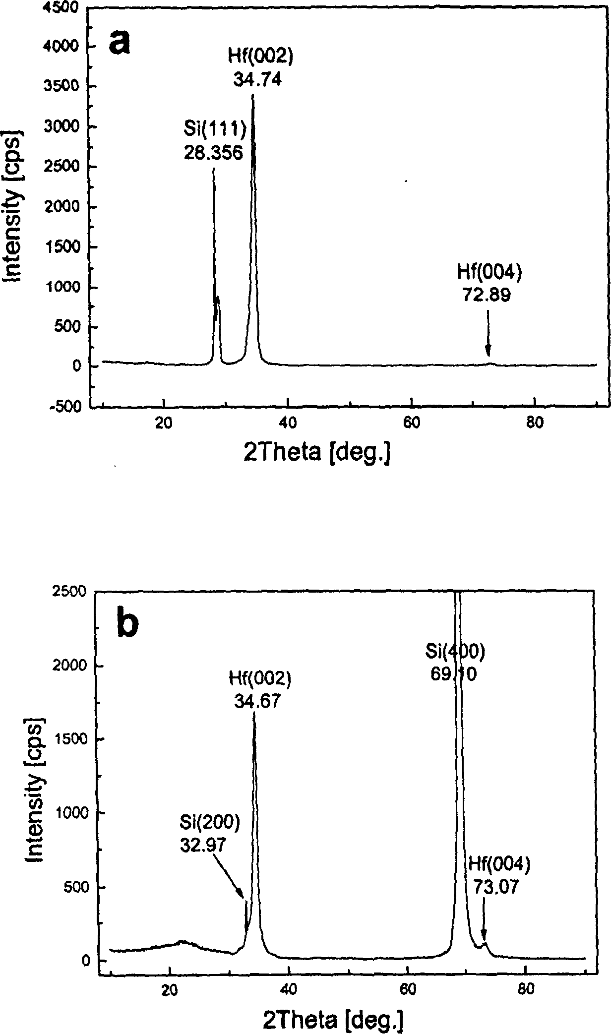
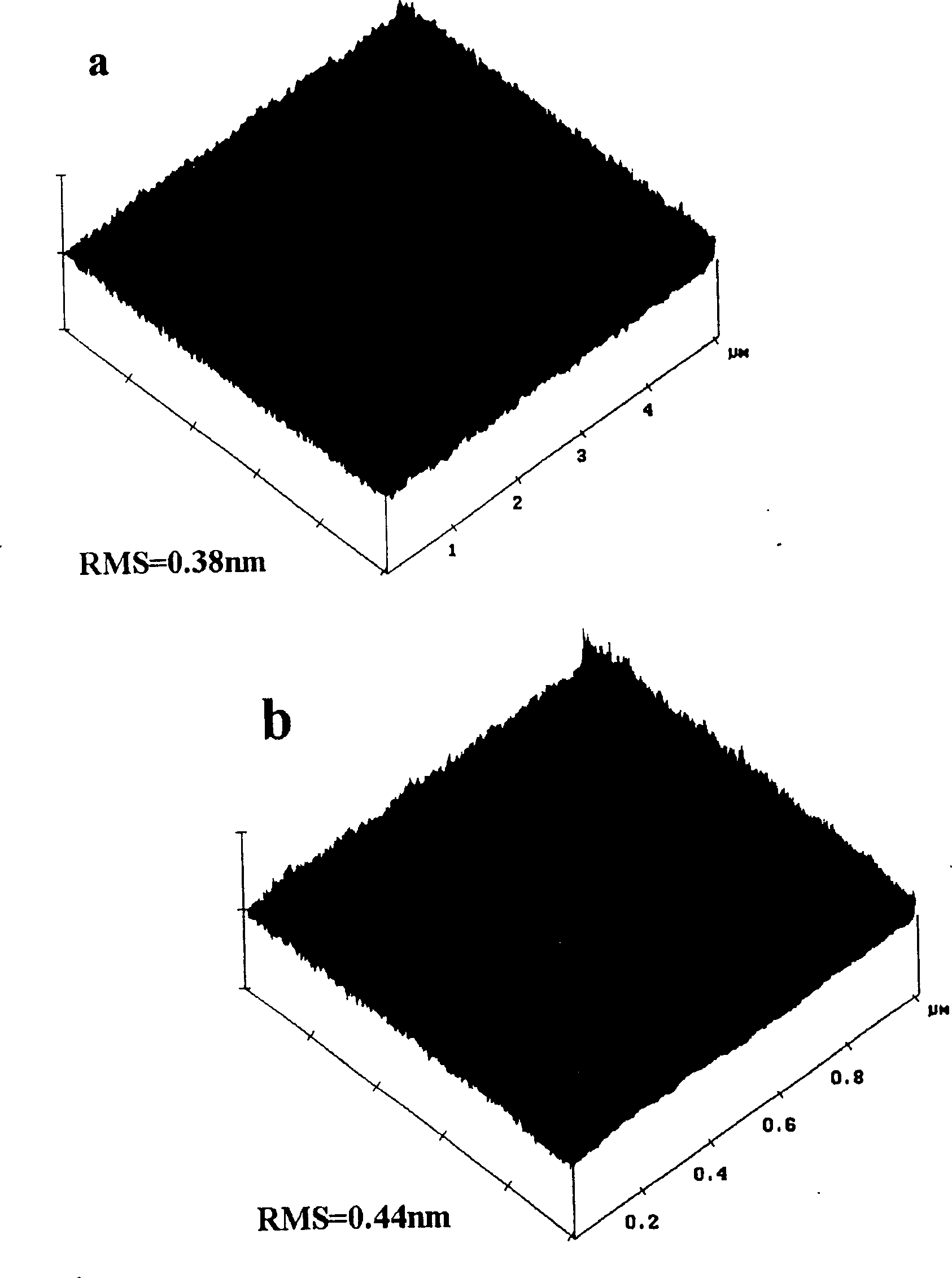
This invention provides a preparation method for hafnium thin film materials. A dual ion beam epitaxy apparatus with the function of mass separation and characteristics of energetic ion deposition is adopted, and in the condition of low purity requirement, low-cost hafnium chloride serves as raw materials is sputtered onto a sanitized substrate with single beam of pure isotopic low-energy argon ions. First, a thin film of hafnium nitride as block layer and buffer layer preventing reactions between substrate and hafnium ion is prepared from consequent pure isotopic low-energy hafnium ion beam and nitrogen ion beam. Next, hafnium film is deposited by means of single pure isotopic low-energy hafnium ion beam epitaxy. By exactly controlling the energy of hafnium ion beam, the amount of deposition agent, beam density, beam shape and deposition temperature, low-cost deposition and low-temperature epitaxy of hafnium which has a high melting point and is difficult to purify can be realized with high purity and high crystallization quality in ultravacuum cultivation room. The preparation method in this invention is convenient to modulate and optimized and is economical for manufacturing hafnium thin films used in semiconductor technology.
Description
Technical field [0001] The present invention belongs to the field of semiconductor technology, and in particular refers to a method for preparing difficult-to-purify and high-melting metal hafnium (Hf) thin film materials on a silicon (Si) substrate using an ion beam epitaxy (IBE) growth device with a double beam structure method. Background of the invention [0002] IVB refractory metals mainly include titanium (Ti), zirconium (Zr) and hafnium (Hf). As important strategic materials, their metals and compounds are widely used in many fields of national economy and national defense construction, especially, With the rapid development of information and electronic technology in recent years, its application in the field of semiconductor technology has attracted more attention. For example, in the field of microelectronics, the scale of ultra-large-scale integrated circuits (ULSI) continues to increase, resulting in the continuous reduction of device feature sizes. This requires fin...
Claims
Login to View More Application Information
Patent Timeline
 IPC IPC(8): C23C14/48C23C14/16C23C14/54C23C14/02
Inventor杨少延柴春林刘志凯陈涌海陈诺夫王占国
OwnerINST OF SEMICONDUCTORS - CHINESE ACAD OF SCI