Inspection system by charged particle beam and method of manufacturing devices using the system

a technology of charged particle beam and manufacturing device, which is applied in the direction of material analysis using wave/particle radiation, photomechanical equipment, instruments, etc., can solve the problems of limited optical resolution, inferior throughput to optical methods, and the use of electron beam methods

Inactive Publication Date: 2002-03-07
EBARA CORP +1
View PDF38 Cites 213 Cited by
  • Summary
  • Abstract
  • Description
  • Claims
  • Application Information

AI Technical Summary

Problems solved by technology

The electron beam method, however, has a weak point in that it is inferior to the optical method in throughput.
It has been known that the resolution of the optical method is limited to {fraction (1 / 2)} of the wavelength of the light to be used, and it is about 0.2 .mu.m in a typical case of visible light being put to practical use.
However, the inspection speed (sometimes also referred to as inspection rate) thereof is very low, and so the development of an inspection apparatus with higher inspection speed has been eagerly anticipated.
Generally, since an inspection apparatus is expensive and the throughput thereof is rather lower as compared to other processing apparatuses, the inspection apparatus has been used after an important process, for example, after the process of etching, film deposition, CMP (Chemical-mechanical polishing) flattening or the like.
This inspection rate, which is extremely low compared to the optical method (not greater than {fraction (1 / 20)}), has been a serious production problem (drawback).
Conventionally, however, there has been no electron beam based defect inspection apparatus which is completed as a general system.
A defect inspection apparatus which applies SEM requires a long time for defect inspection.
In addition, increasing the beam current to improve throughput would cause a degradation of the beam due to the space-charge effect and charging on the wafer with insulating material formed on the surface thereof, thereby failing to produce satisfactory SEM images.
However, since the high voltage is applied to the objective lens, while the negative voltage is applied to the sample, there has been a risk that an electric discharge may occur between the objective lens and the sample.
Further, in the electron microscope in the prior art, even in the case where no negative voltage is applied to the sample, if there is a great potential difference between the objective lens and the sample, then it is again feared that the electric discharge may occur between the objective lens and the sample.
Still further, if the voltage applied to the objective lens is set lower in order to deal with a possible electric discharge to the sample, the electrons aren't sufficiently energized, resulting in a poor resolution.
Through a series of these positive feedback, eventually an electric discharge occurs between the objective lens and the semiconductor wafer and damages the pattern or the like on the semiconductor wafer, which has been problematic in the prior art.
In the case where an E.times.B separator having such a configuration as described above has been applied to a defect inspection apparatus such as a projective electron beam inspection apparatus, there has been a problem of efficiency in inspection in that the irradiated region of the electron beam cannot be enlarged, in order to perform a precise inspection.
However, the above defect inspection apparatus in the prior art has been problematic in that the irradiation of the electron beam causes the surface of the sample to be charged, and carriers from this charging cause a distortion in the image data, which makes it difficult to detect any defects accurately.
When alternatively the electron beam current is reduced to make the distortion by the carriers small enough to resolve the problem of said distortion in the image data, the S / N ratio for the secondary electron signal is adversely affected, so that the possibility of invalid error detection is increased, which has been another problem.
Further, it has also been a problem in the prior art that multiple scanning and averaging processes for improving the S / N ratio causes a decrease in throughput.
However, this type of imaging apparatus according to the prior art, including the above-described apparatus that has been disclosed in the publication, has been problematic in that the potential distribution on the surface of the substrate or the object to be inspected is not necessarily uniform and the contrast of the image is insufficient, which may cause distortion.
However, if the electron beam is irradiated on the surface in a relatively large area of the sample wafer of the real device, due to the sample surface being made of an insulating material such as silicon dioxide or silicon nitride, the electron beam irradiation against the sample surface and associated emanation of secondary electrons from the sample surface causes the sample surface to be positively charged, and an electric field produced by this potential has problematically caused a variety of image disorders in the secondary electron beam image.
Because of this gas supply cycle, every time when the stage moves, it has happened that the vacuum level in the chamber C is lowered, which has caused such problems that the exposure, inspection, or processing with the charged particles beam described above could not be carried out stably, and the sample might be contaminated.
Also, in the conventional stage including a combination of the hydrostatic bearing and the differential exhausting mechanism shown in FIG. 55, there have been such problems that because of the differential exhausting mechanism having been added, the structure has become more complicated and its reliability as a stage has decreased while its cost has increased over that of a stage having a hydrostatic bearing used in the atmospheric pressure.
However, there has been such a problem associated with the prior art described above, which is that a position mismatch occurs between the image of the secondary electron beam obtained upon irradiating the primary electron beam against the region to be inspected in the sample surface and the reference image prepared in advance, which decreases the accuracy in defect detection.
This position mismatch becomes a serious problem especially when the irradiation region of the primary electron beam is offset to the wafer resulting in the inspection pattern partially being out of the detection image of the secondary electron beam, which could not be handled only with the technology for optimizing a matching region within the detection image.
This problem could be a fatal drawback especially in the inspecting of patterns of high precision.
Problems in this projecting method are; (1) a charge build-up is more likely to occur in the surface of a sample due to an in-block irradiation of electron beam; and (2) an electron current obtained by this method is limited (up to about 1.6 .mu.A), which prohibits any improvement in inspection rate.
(b) It is almost impossible for gas desorbed or leaked from the hydrostatic bearing to go though the divider and reach the space for the charged particle beam irradiating system.

Method used


Image

  • Inspection system by charged particle beam and method of manufacturing devices using the system
  • Inspection system by charged particle beam and method of manufacturing devices using the system
  • Inspection system by charged particle beam and method of manufacturing devices using the system

Examples


second embodiment

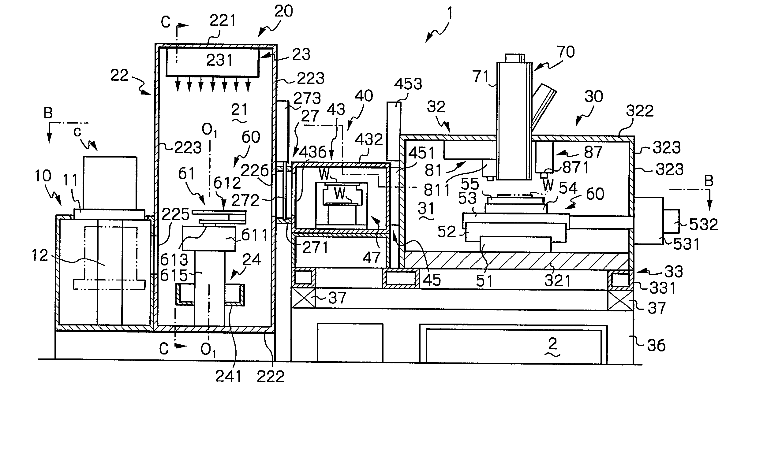
[0466] FIG. 19 shows a precharge unit of the present invention. FIG. 19 shows an irradiation source of such type that irradiates an electron beam as a charged particle beam. The irradiation source comprises a hot filament 821, a deriving electrode 824, a shield case 826, a filament power supply 827, and an electron deriving power supply 823. The deriving electrode 824 is 0.1 mm in thickness, has a slit 0.2 mm wide and 1.0 mm long, and is arranged relative to the filament 821 of a diameter of 0.1 mm so as to take the form of a three-electrode type electron gun. The shield case 826 is also provided with a slit of 1 mm wide and 2 mm long, and is assembled so that the shield case 826 is spaced from the deriving electrode 824 by 1 mm with its slit center being aligned with the slit center of the deriving electrode 824. The filament is made of tungsten (W), and it is found that an electron current of in the order of .mu.A can be obtained with a current of 2 A being supplied to the filamen...

third embodiment

[0468] FIG. 20 shows a precharge unit of the present invention. FIG. 20 shows an irradiation source of a type that irradiates ions 829 as a charged particle beam. This irradiation source comprises a filament 821, a filament power supply 822, an electric discharge power supply 827, and an anode shield case 826, in which both of anode 828 and the shield case 826 have the same sized slit of 1 mm.times.2 mm respectively formed therethrough, and they are assembled so that the centers of both slits are aligned with each other. Ar gas 830 is introduced into the shield case 826 through a pipe 831 with about 1 Pa and this irradiation source is operated by way of an arc discharge caused by the hot filament 821. The bias voltage is set to a positive value.

fourth embodiment

[0469] FIG. 21 shows a plasma irradiation type of a precharge unit according to the present invention. It has the same structure as that of FIG. 20. The operation thereof, similarly to the above description, is made effective by way of the arc discharge by the hot filament 821, in which by setting the bias potential to 0V, the plasmas 832 are forced by gas pressure to effuse through the slit to be irradiated onto a sample substrate. Since in the plasma irradiation method, the beam is composed of a group of particles that has both positive and negative charges, which is different from the other irradiation methods, it allows both positive and negative surface potentials in the surface of the sample substrate to approach zero.

[0470] A charged particle irradiating section 819 arranged in the proximity of the sample substrate W has a configuration as illustrated in any of FIGS. 18 to 21, which is designed to irradiate charged particles 818 onto the sample substrate with a suitable condi...


PUM

PropertyMeasurementUnit
energyaaaaaaaaaa
energyaaaaaaaaaa
wavelengthaaaaaaaaaa

Abstract

An inspection apparatus by an electron beam comprises: an electron-optical device 70 having an electron-optical system for irradiating the object with a primary electron beam from an electron beam source, and a detector for detecting the secondary electron image projected by the electron-optical system; a stage system 50 for holding and moving the object relative to the electron-optical system; a mini-environment chamber 20 for supplying a clean gas to the object to prevent dust from contacting to the object; a working chamber 31 for accommodating the stage device, the working chamber being controllable so as to have a vacuum atmosphere; at least two loading chambers 41, 42 disposed between the mini-environment chamber and the working chamber, adapted to be independently controllable so as to have a vacuum atmosphere; and a loader 60 for transferring the object to the stage system through the loading chambers.

Description

[0001] 1. Field of the Invention[0002] The present invention relates to an electron beam based inspection apparatus for inspecting defects in patterns formed on the surface of an object to be inspected, and more particularly, to an inspection apparatus useful, for example, in inspecting defects on a wafer in a semiconductor manufacturing process, which includes irradiating an object to be inspected with an electron beam, detecting secondary electrons which vary in accordance with the properties of the surface thereof to form image data, and inspecting patterns formed on the surface of the object to be inspected based on the image data at a high throughput, and a method of manufacturing devices at a high yield rate using the inspection apparatus. More specifically, the invention relates to a projection type electron beam inspection apparatus which adopts a area beam and a method of manufacturing devices using the inspection apparatus.[0003] 2. Field of the Invention[0004] In semicond...

Claims


Application Information

Patent Timeline
Patent Type & Authority Applications(United States)
IPC IPC(8): G01N23/225H01J37/06H01J37/073H01J37/18H01J37/20H01J37/22H01J37/244H01J37/28
CPCG01N23/225H01J37/266H01J37/073H01J37/185H01J37/20H01J37/222H01J37/244H01J37/28H01J2237/082H01J2237/202H01J2237/20228H01J2237/204H01J2237/22H01J2237/24564H01J2237/2806H01J2237/2816H01J2237/2817H01L21/6719H01L21/67213G01N23/2251G01N23/227H01J29/70H01J37/141H01J37/06
Inventor NAKASUJI, MAMORUNOJI, NOBUHARUSATAKE, TOHRUHATAKEYAMA, MASAHIROKIMBA, TOSHIFUMISOBUKAWA, HIROSIYOSHIKAWA, SHOJIMURAKAMI, TAKESHIWATANABE, KENJIKARIMATA, TSUTOMUOOWADA, SHINSAITO, MUTSUMIYAMAZAKI, YUICHIRONAGAI, TAKAMITSUNAGAHAMA, ICHIROTA
Owner EBARA CORP
Why Eureka
Try Eureka