Electroluminescent display formed on glass with a thick film dielectric layer

a technology of dielectric layer and glass, which is applied in the direction of discharge tube luminescnet screen, discharge tube/lamp details, electric discharge lamps, etc., can solve the problems of premature electrical breakdown limited thickness of the dielectric layer, and different constraints on the deposition equipment and surrounding cleanliness

Inactive Publication Date: 2002-09-12
UNIVERSITY OF CINCINNATI
View PDF0 Cites 21 Cited by
  • Summary
  • Abstract
  • Description
  • Claims
  • Application Information

AI Technical Summary

Benefits of technology

0007] The present invention is premised on the realization that with proper selection of material and implementation of phosphor and dielectric material, an electroluminescent device utilizing a thick film dielectric layer can be formed on and emit through a glass substrate. More particularly the present invention is premised on the realization that high temperature stable phosphor

Problems solved by technology

As such, the thickness of the dielectric layers is generally limited.
Due to the thinness of such dielectric layers any irregularities such as pinholes can result in premature electrical breakdown of the dielectric layers.
This requirement for an irregularity-free thin film places different constraints on the deposition equipment and surrounding cleanliness if adequate yields are to be achieved.
However, this sintering of the dielectric layer gener

Method used


Image

  • Electroluminescent display formed on glass with a thick film dielectric layer
  • Electroluminescent display formed on glass with a thick film dielectric layer
  • Electroluminescent display formed on glass with a thick film dielectric layer

Examples


example 1

[0028] Dupont 9970 Ag:Pt paste was screen printed onto alumina substrates, dried, and fired at 850.degree. C. for ten minutes. One or two layers of Dupont 5540 dielectric paste were screen printed, dried and sintered at 850.degree. C. for ten minutes. The 5540 paste contains barium titanate along with glass or fluxing agents that facilitate lower temperature (<900.degree. C.) sintering of the dielectric. A scanning electron microscope photograph showed that the thick-film dielectric layer has a surface roughness of .about.1 micron and is granular with high porosity. The resulting dielectric layer thickness was 20-40 microns with a permittivity of .epsilon..about.6000. A GaN:Er phosphor film of .about.1 micron thickness was then deposited by solid-source molecular beam epitaxy onto the dielectric / metal / ceramic substrates. .about.300 nm thick indium-tin-oxide transparent electrodes were then sputtered through a stencil mask onto the GaN:Er phosphor film. The resulting structure was bi...

example 2

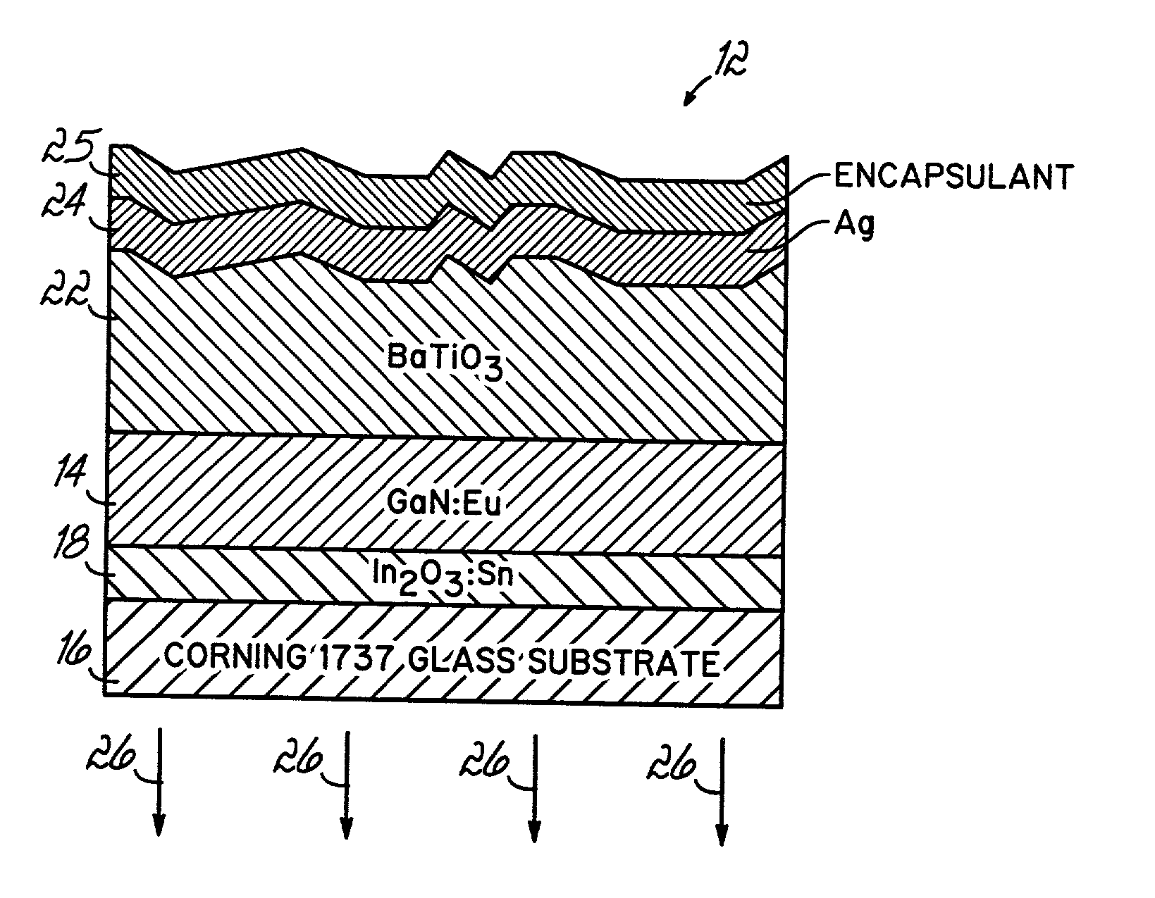
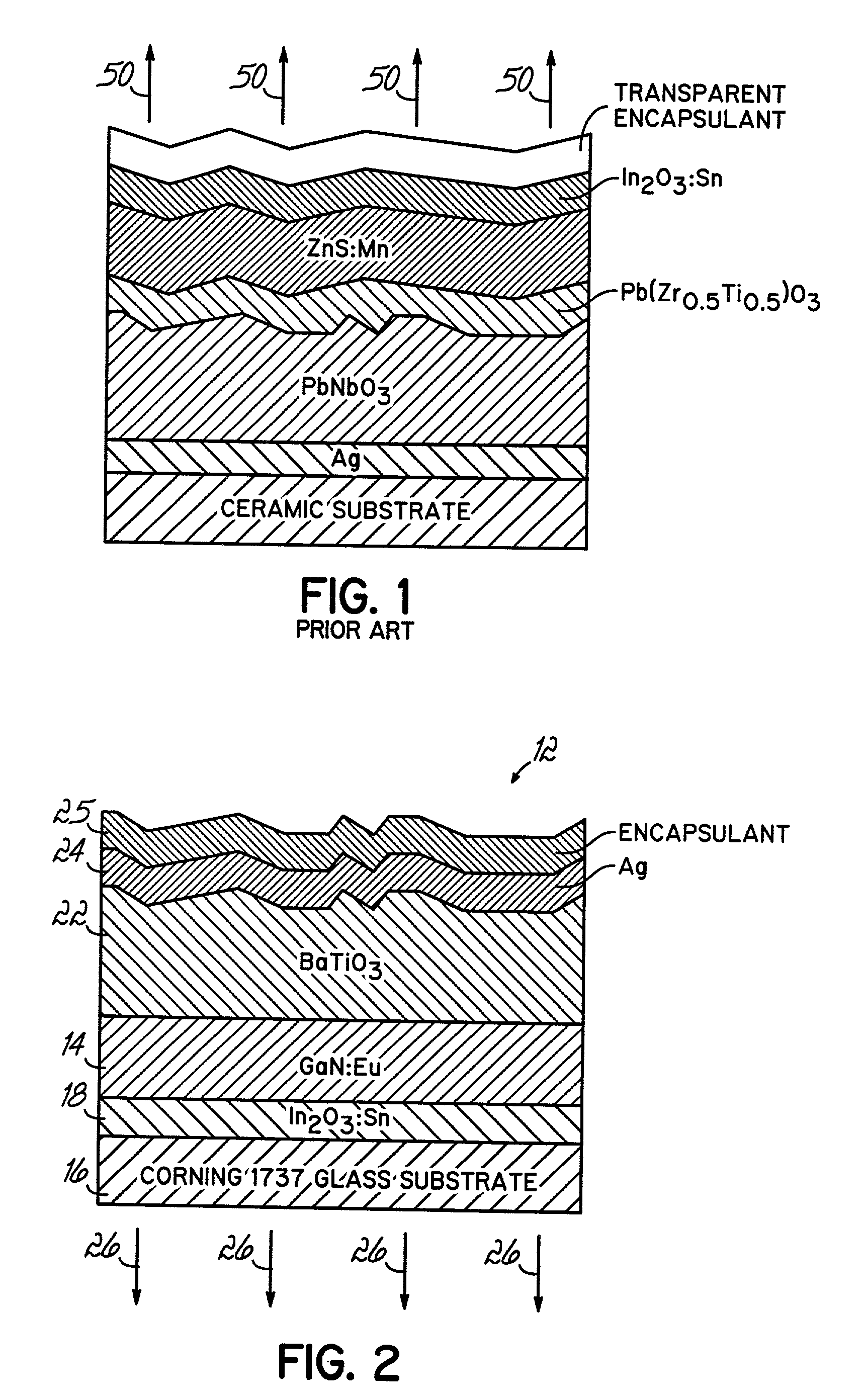
[0029] .about.300 nm indium-tin-oxide films were deposited on Corning 1737 glass substrate which has a thermal strain point of 666.degree. C., sufficiently above the .about.600.degree. C. substrate temperature used during gallium nitride phosphor deposition. Corning 1737 is a widely utilized display glass due to its compatibility with low temperature (500-600.degree. C.) poly-Si processing used for active-matrix liquid crystal displays. Approximately 1 micron thick erbium doped gallium nitride phosphor film was deposited by solid-source molecular beam epitaxy onto the indium-tin-oxide coated 1737 glass substrates. Following phosphor deposition, 1 layer of Dupont 5540 dielectric paste was screen printed, dried, densified for 10 minutes at .about.600.degree. C., and sintered at .about.800.degree. C. for 4 minutes. The resulting dielectric layer had a thickness of .about.20 microns, breakdown strength >200 V, and permittivity of .epsilon..about.500-1000. Rear electrodes were formed by ...

example 3

[0031] A device similar to that of Example 2 was formed with the following changes to fabrication of the thick-film dielectric layer. Following the phosphor deposition, 1 layer of Dupont 5540 dielectric paste was screen printed, dried, densified for 1 minutes at .about.600.degree. C. A second layer of Dupont 5540 dielectric paste was then screen printed, dried, and densified for 10 minutes at .about.600.degree. C. This stock of two dielectric layers was then sintered at .about.800.degree. C. for 4 minutes. The resulting dielectric layer had a thickness of .about.40 microns, breakdown strength >300 V, and permittivity of .epsilon..about.500-1000. The device exhibited similar luminance characteristics to that of Example 2 but showed improved reliability at high voltages (>300 V breakdown).


PUM


Abstract

Wide band gap semiconductor materials doped with rare earth form alternating current electroluminescent devices. The semiconductors are preferably gallium nitride, indium nitride or aluminum nitride and the electric luminescent device may have an upper and lower thin coat of a dielectric material in turn connected to alternating current electrodes. In a preferred embodiment, the electroluminescent device is formed on a glass substrate coated with a thick film of dielectric. The dielectric can be applied as a gel and heat treated after coating the semiconductor material to form a light emitting device.

Description

BACKGROUND OF THE INVENTION[0001] The next generation of flat panel displays is seeking to provide advances in brightness, efficiency, color, purity, resolution, scalability, reliability and reduced costs. One such technology is thin film electroluminescence (TFEL) inorganic phosphors. TFEL displays can provide high brightness, outstanding durability and reliability. Current inorganic TFEL phosphors are composed of group II-VI wide band gap semiconductor hosts such as zinc sulfide and strontium sulfide which provide hot carriers (greater than two electron volts) which impact luminescent centers such as manganese, cerium, and copper.[0002] Sufficient hot carrier generation requires high field strength exceeding the break down field of the phosphor thin film. An alternating current biased dielectric / phosphor / dielectric layered structure allows reliable high field operation by current limiting of the electrical breakdown of the phosphor layer. Generally these dielectric layers are thin...

Claims


Application Information

Patent Timeline
IPC IPC(8): H01L33/30H01L33/32H05B33/10H05B33/12H05B33/14
CPCH01L33/305H01L33/32H05B33/10H05B33/12H05B33/145
Inventor STECKL, ANDREW J.HEIKENFELD, JASON C.
Owner UNIVERSITY OF CINCINNATI
Why Eureka
Try Eureka