Method of forming crystalline semiconductor thin film on base substrate, lamination formed with crystalline semiconductor thin film and color filter

a technology of crystalline semiconductor and thin film, applied in the direction of crystal growth process, instrumentation, vacuum evaporation coating, etc., can solve the problems of increasing the cost in view of economics, the inability to form the photoconductor thin film by this method on the plastic substrate to be described later, and the need for an expensive apparatus

Inactive Publication Date: 2002-09-19
FUJIFILM BUSINESS INNOVATION CORP
View PDF0 Cites 3961 Cited by
  • Summary
  • Abstract
  • Description
  • Claims
  • Application Information

AI Technical Summary

Problems solved by technology

In the methods described above, the method of forming a photosemiconductor thin film by sintering the amorphous titanium dioxide film requires heating of the substrate at a high temperature for a long time, which increases the cost in view of economy.
Further, formation of the photoconductor thin film by this method on a plastic base material to be described later is actually impossible in view of the heat resistance of the plastic substrate.
Further, while the RF sputtering method is excellent as a method of obtaining an anatase titanium dioxide of high photovoltaic activity, it is necessary to use an expensive apparatus and it is difficult to manufacture the photoconductor thin film at a reduced cost by this method Although some of plastic base materials have heat resistance of 250.degree. C., those having heat resistance of 250.degree. C. and also having transparency and available at a reasonable cost have not yet been known at present.
The former liquid crystal display panel involves the problem in that an exposure mask is required upon manufacture of the color filter and error tends to occur in the accuracy of the positional alignment between both of the driving and filter substrates to lower the display quality or production yield.
However, the latter method leads to increase cost since it is necessary to make the color filter conductive by using through holes or the like.
Generally, for the flexible substrates for the liquid crystal use, plastic materials having transparency and high heat resistance and excellent in gas barrier property have been demanded, but the heat resistance is only about at 223.degree. C. even in polyether sulfone (PES) which is considered to have the highest heat resistance, so that it is difficult to dispose the photosemiconductor thin film described above on the plastic substrate and formation of the color filter by the photo-electrodeposition method on the plastic substrate has not yet been attained commercially.
This is because a high temperature processing step is necessary for forming a polycrystal semiconductor thin film at high carrier concentration used in TFT and manufacture of the TFT driving circuit on the plastic substrate is impossible at present.
While the inkjet method has an advantage of not including a photolithographic step, it tends to cause color mixing and poor in view of the resolution and the positional accuracy.
Further, since the electrodeposition method requires formation of an electrode corresponding to a pixel, the pattern shape is restricted to a stripe pattern or the like and cannot be used for the liquid crystal panel provided with a TFT driving circuit.
Further, manufacture of the TFT driving circuit to the plastic substrate is impossible at present as described above but there is a strong demand for the liquid crystal display panel using the plastic substrate provided with the TFT circuit.
Accordingly, the methods described above cannot crystallize the entire amorphous layer.
Further, they require another step of providing the thermobarrier layer and also requires an expensive laser beam irradiation device.
In addition, since it is necessary to scan the laser beam spot over the entire film, they also involve a disadvantage that it is difficult to increase the area of the film and take a long time for crystallizing the entire area.

Method used


Image

  • Method of forming crystalline semiconductor thin film on base substrate, lamination formed with crystalline semiconductor thin film and color filter
  • Method of forming crystalline semiconductor thin film on base substrate, lamination formed with crystalline semiconductor thin film and color filter
  • Method of forming crystalline semiconductor thin film on base substrate, lamination formed with crystalline semiconductor thin film and color filter

Examples


example 1

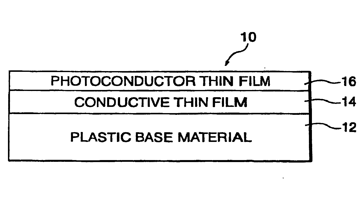
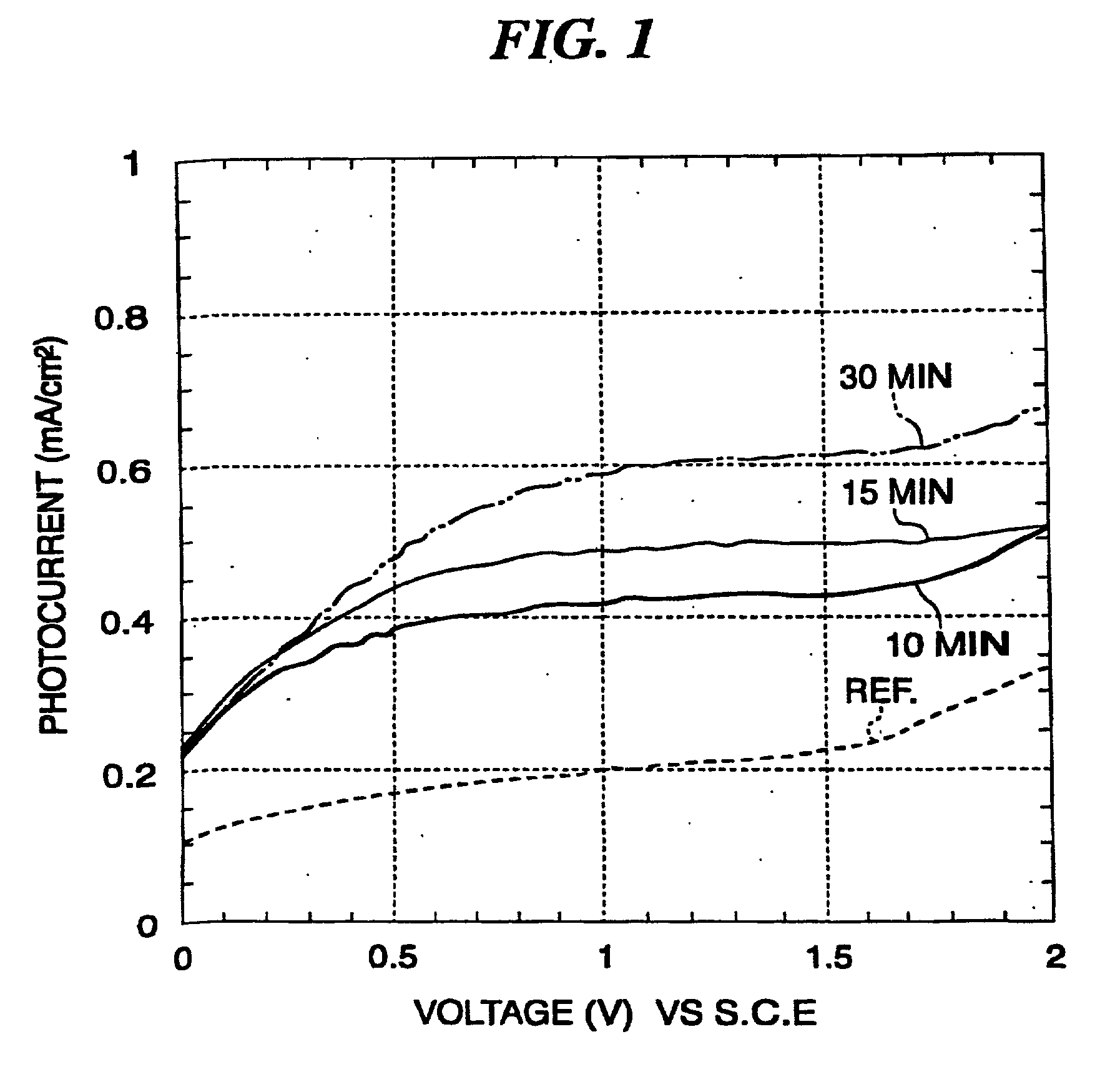
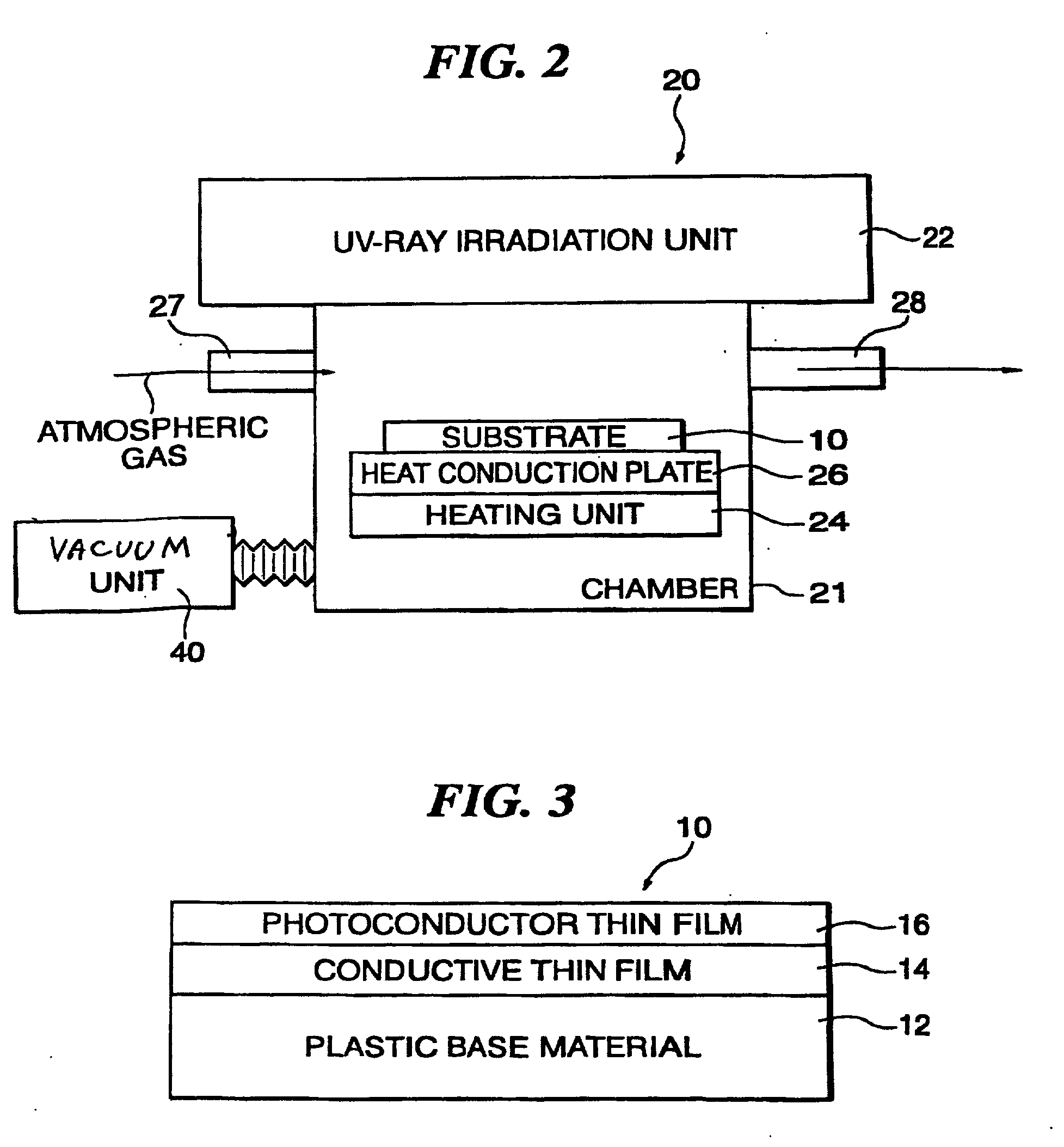
[0087] To a non-alkali glass substrate of 0.7 mm thickness (Corning 1737 glass), amorphous titanium dioxide was deposited at a film thickness of 200 nm at a substrate temperature of 180.degree. C. using an RF sputtering method. Then, using an experimental device as shown in FIG. 2 having an inner capacity of about 1 liter), after previously removing oxygen by a vacuum treatment (to 10.sup.-2 Pa), the glass substrate formed with titanium dioxide was heated to 150.degree. C. in a high purity nitrogen gas atmosphere containing 3% hydrogen gas (flow rate: 1 l / min, atmospheric pressure), and UV-rays (wavelength: 172 nm, light intensity: 10 mW / cm.sup.2) were applied for 10 minutes by an excimer lamp (manufactured by Ushio, Inc.) while keeping the temperature.

[0088] When the X-ray diffraction intensity of the resultant annealed film was examined. A diffraction peak was observed at 2.theta. of 25.260. Further, as a result of examination for the angle of contact of the film, it was 1.5.degre...

example 2

[0090] On a plastic sheet of 0.1 mm thickness (PES mm, manufactured by SUMITOMO BAKELITE), an annealed film was formed on the plastic sheet in the same manner as in Example 1 except for changing the temperature for the annealing treatment to 125.degree. C.

[0091] When the X-ray diffraction intensity of the resultant annealed film was examined. A diffraction peak was observed at 2.degree. of 25.260. Further, as a result of examination for the angle of contact of the films it was 2.5.degree. and it was observed that the surface was strongly hydrophilic.

[0092] The result described above supports that amorphous titanium oxide was converted into crystalline titanium oxide (photoconductor) by the annealing treatment.

example 3

[0093] A crystalline titanium oxide thin film was formed on a plastic sheet in the same manner as in Example 2 except for changing the temperature for the annealing treatment to 50.degree. C. and the UV-ray irradiation time to five hours.

[0094] The resultant thin film showed the same nature as that in Example 2.


PUM

PropertyMeasurementUnit
temperatureaaaaaaaaaa

Abstract

A method of forming a crystalline semiconductor thin film on a base material which can be prepared at a low temperature by simple step and device, the method including a processing step of applying UV-rays to an amorphous semiconductor thin film provided on a base material while keeping a temperature at not less than 25° C. and not more than 300° C. in a vacuum or a reducing gas atmosphere, as well as a substrate having the semiconductor thin film provided on the base material, a substrate for forming a color filter and a color filter using the substrate.

Description

[0001] 1. Field of the Invention[0002] This invention concerns a method of forming a crystalline semiconductor thin film on a substrate, a lamination formed with a crystalline semiconductor thin film on a substrate, a lamination for use in a substrate provided with a transparent conductive thin film and a transparent semiconductor thin film used for production of various kinds of display devices such as CCD cameras or liquid crystal display devices or camera image sensors, particularly, for the color filter suitable to portable terminals such as portable telephones or small personal computers, as well as color filters manufactured by using the substrate.[0003] 2. Description of the Related Art[0004] Photoconductors having catalytic activity or photovoltaic activity have been noted for their specific applications in recent years. For example, titanium dioxide as a photosemiconductor is said to oxidatively decompose organic contaminants deposited on the surface, air contaminating subs...

Claims


Application Information

Patent Timeline
Patent Type & Authority Applications(United States)
IPC IPC(8): G02B5/20C23C14/08C23C14/34C23C14/58G02F1/1335H01L21/20
CPCC23C14/083C23C14/58H01L21/2022H01L21/02565H01L21/02422H01L21/02491H01L21/02667H01L21/02631H01L21/02628G02F1/1335H01L21/02686
Inventor OHTSU, SHIGEMISHIMIZU, KEISHIYATSUDA, KAZUTOSHIAKUTSU, EIICHI
Owner FUJIFILM BUSINESS INNOVATION CORP
Why Eureka
Try Eureka