

Opaque low resistivity silicon carbide
a technology of silicon carbide and low resistivity, which is applied in the field of opaque, low resistivity silicon carbide, can solve the problems of restricting its use in other applications, high resistivity restricting its use in fabricating components that require a greater degree of electrical conductivity, and restricting its use in applications. , to achieve the effect of low resistivity, low resistivity and low resistan
- Summary
- Abstract
- Description
- Claims
- Application Information
AI Technical Summary
Benefits of technology
Problems solved by technology
Method used
Image

Examples
example 1
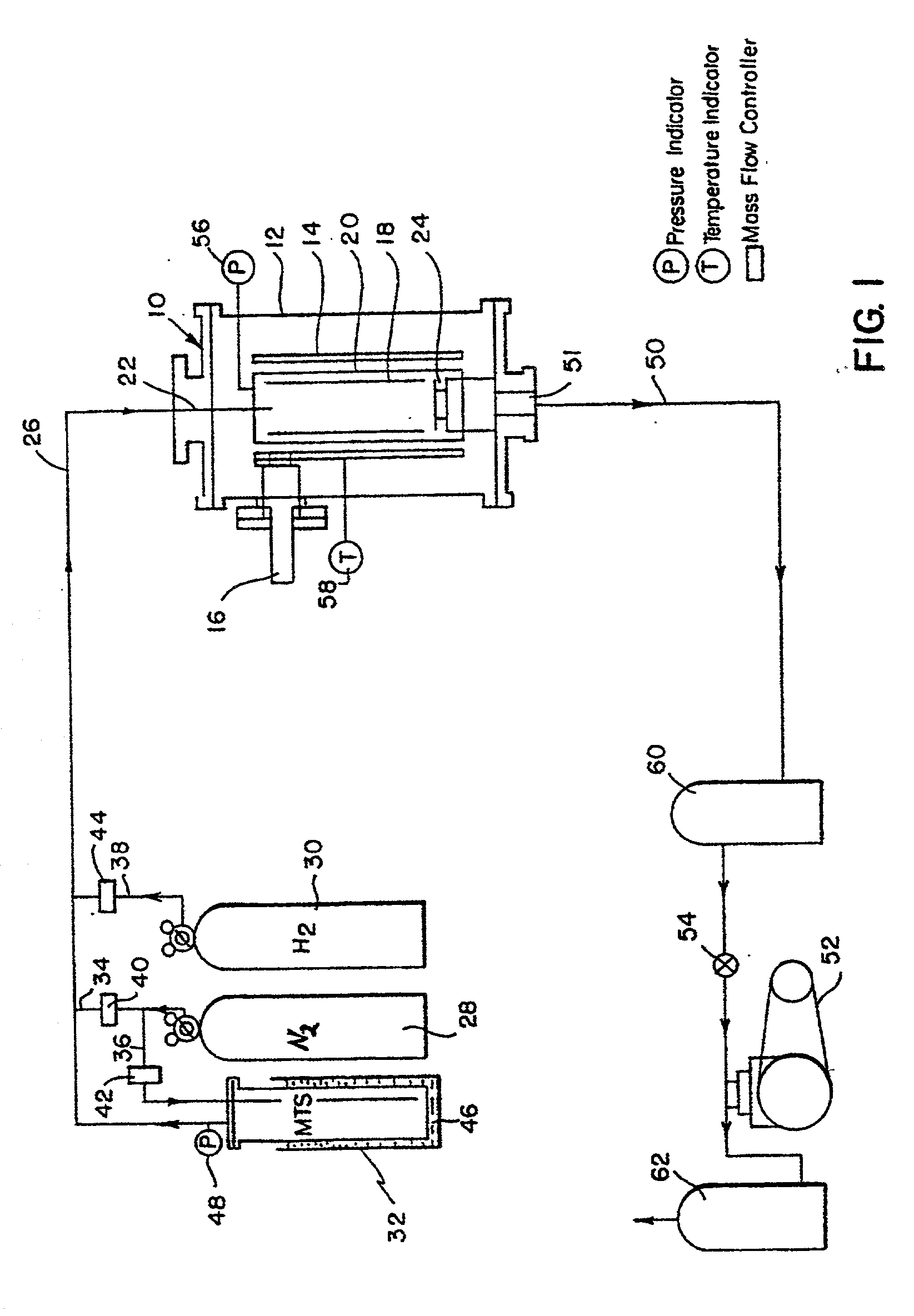
[0041] Free-standing opaque, low resistivity silicon carbide was prepared in an apparatus similar to the apparatus illustrated in FIG. 1. Deposition temperature in the CVD chamber was about 1350.degree. C. and pressure was about 200 torr. Hydrogen partial pressure was about 90 torr, nitrogen partial pressure was about 93 torr (a nitrogen content of about 46.5% by volume of the CVD chamber), and MTS partial pressure was about 17 torr. No inert or noble gases were employed in the CVD process. Silicon carbide was deposited onto a graphite mandrel coated with a release agent. The deposition process was performed over about 48 hours. The process produced an edge ring that was opaque to light at a wavelength range of from about 0.7 .mu.m to about 0.95 .mu.m at temperatures of about 300.degree. C. and higher.
[0042] A control free-standing silicon carbide bulk material was also prepared. The control free-standing silicon carbide was prepared by the same process as described above except tha...
example 2
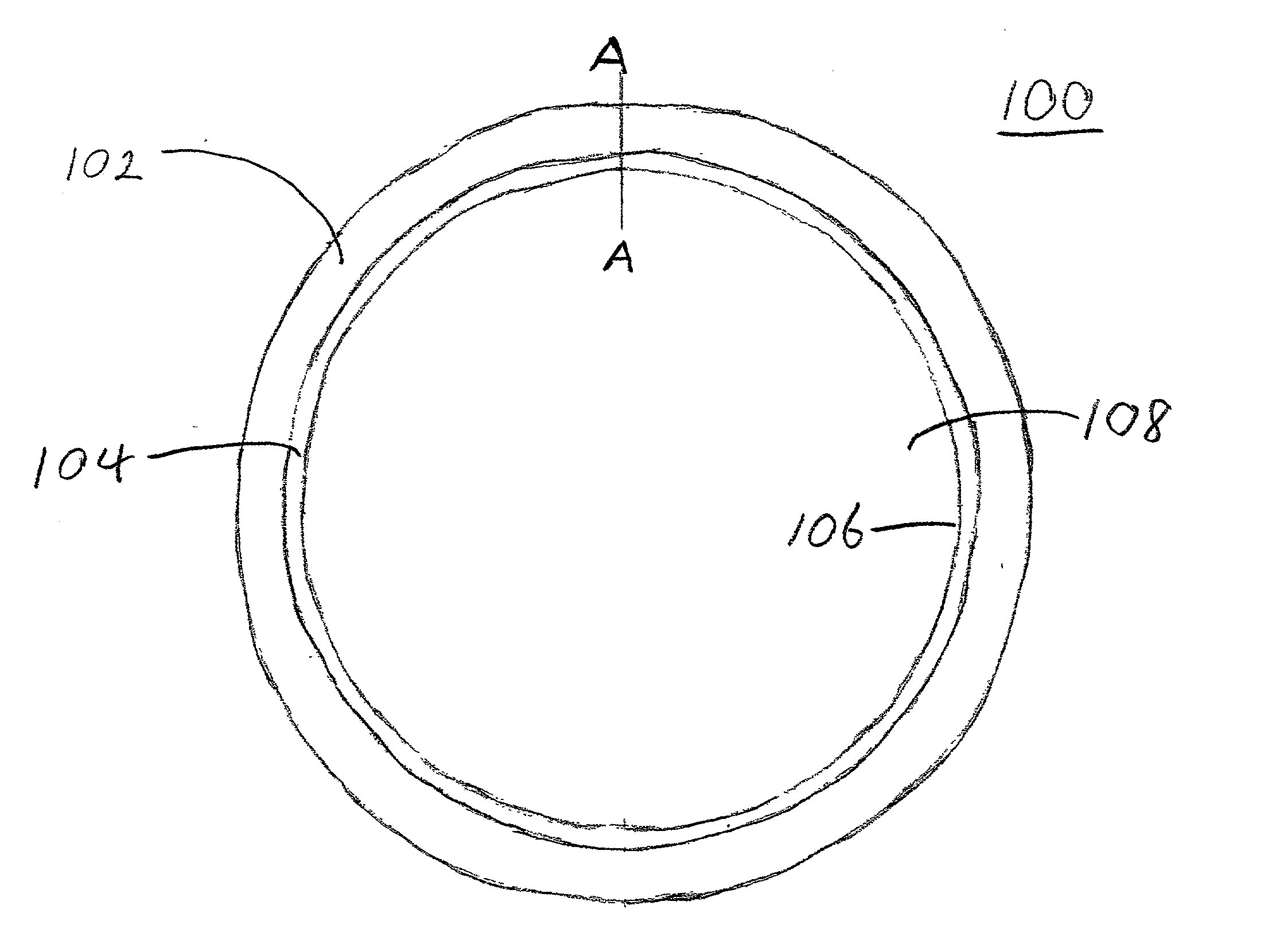
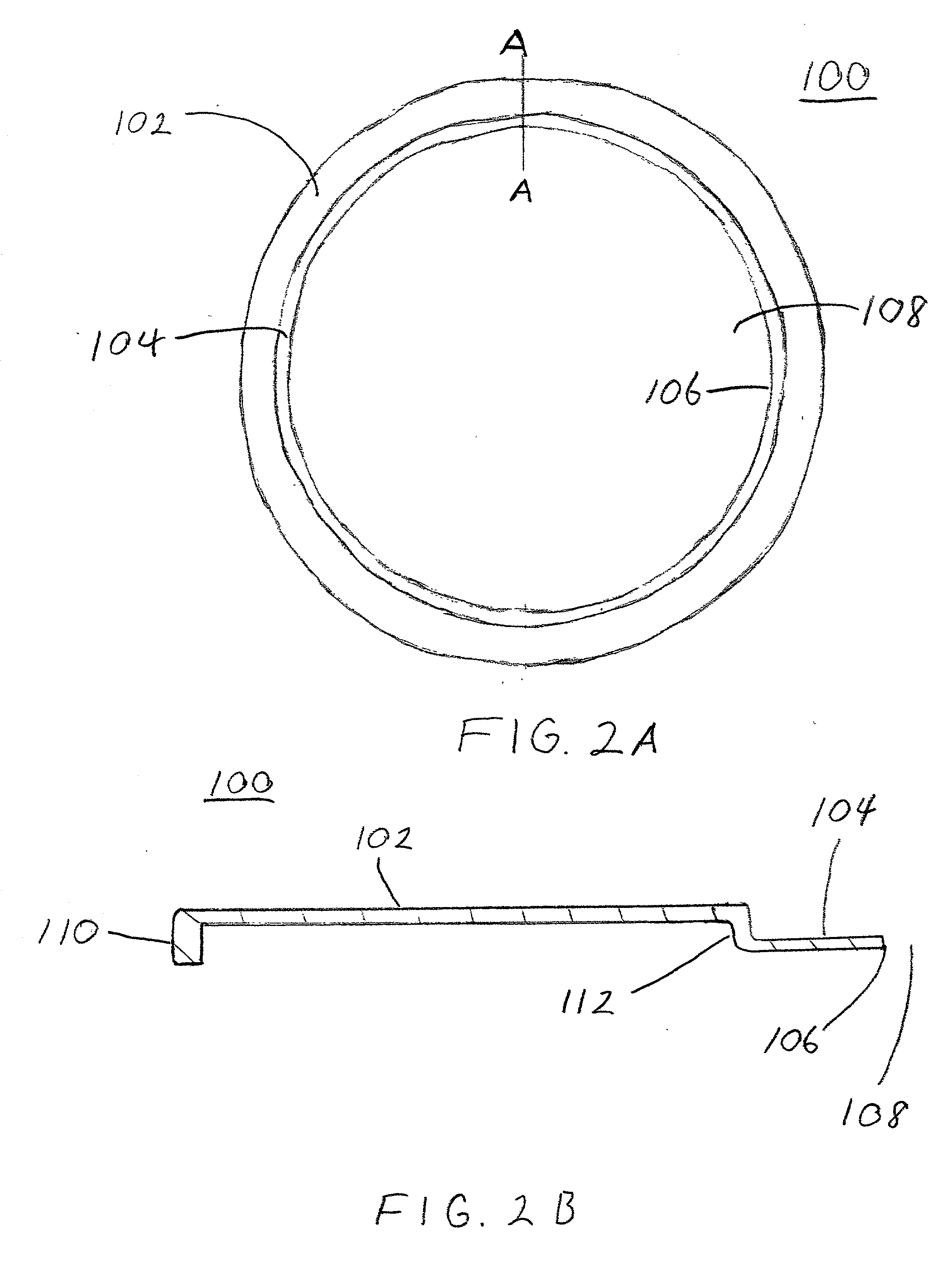
[0048] A free standing opaque, silicon carbide edge ring having a shape similar to the edge ring illustrated in FIGS. 2A and 2B was prepared by the same process as in Example 1 above with a high concentration nitrogen atmosphere. As in Example 1 above, the bulk resistivity of the edge ring was measured at four locations and ranged from about 0.009 to about 0.015 ohm-cm. The edge ring had about a 30% lower thermal mass than the edge ring in Example 1 because its thickness was about 0.25 mm versus about 0.36 mm for the edge ring in Example 1 and there was no poly-silicon coating. The low resistivity silicon carbide edge ring was opaque to light at a wavelength of from about 0.7 .mu.m to about 0.95 .mu.m at a temperature of about 300.degree. C. and higher.
[0049] A silicon wafer was placed in the edge ring and the assembly was placed into an RTP Radiance.RTM. for similar thermal testing as in Example 1. The temperature of the RTP chamber went from about 20.degree. C. to about 1200.degre...
PUM
| Property | Measurement | Unit |
|---|---|---|
| temperature | aaaaa | aaaaa |
| temperature | aaaaa | aaaaa |
| temperature | aaaaa | aaaaa |
Abstract
Description
Claims
Application Information