Multilayer thin film hydrogen getter

a hydrogen getter and thin film technology, applied in the field of thin film hydrogen getters, can solve the problems of reducing the performance and reliability of gallium arsenide (gaas) integrated circuits which are hermetically packaged, unable to re-work the assembly, and unable to return false results, etc., to achieve excellent high electrical conductance metals, enhance circuit performance, and cost benefits

Inactive Publication Date: 2003-04-03
RAYTHEON CO
View PDF4 Cites 27 Cited by
  • Summary
  • Abstract
  • Description
  • Claims
  • Application Information

AI Technical Summary

Benefits of technology

0014] The palladium continues to prevent the titanium from being oxidized once the getter is exposed to the atmosphere, while the metal film below, e.g., aluminum or copper, provides an excellent high electrical conductance metal for ground shield. The getter acts to absorb hydrogen, as described above. In addition to the advantages described above for the getter, t

Problems solved by technology

Gallium Arsenide (GaAs) integrated circuits which are hermetically packaged will suffer from reduced performance and reliability if the hydrogen that is evolved from the packaging materials is allowed to diffuse into the GaAs devices.
There are several disadvantages to this getter: (1) in order to provide enough hydrogen absorption capacity in a package, a significant volume of silicone getter must be used; (2) Residual Gas Analysis (RGA), used to determine internal contaminants within a hermetic package, can return false results related to moisture content when the silicone product is used; (3) silicone oil migration within the package has b

Method used


Image

  • Multilayer thin film hydrogen getter
  • Multilayer thin film hydrogen getter
  • Multilayer thin film hydrogen getter

Examples


first embodiment

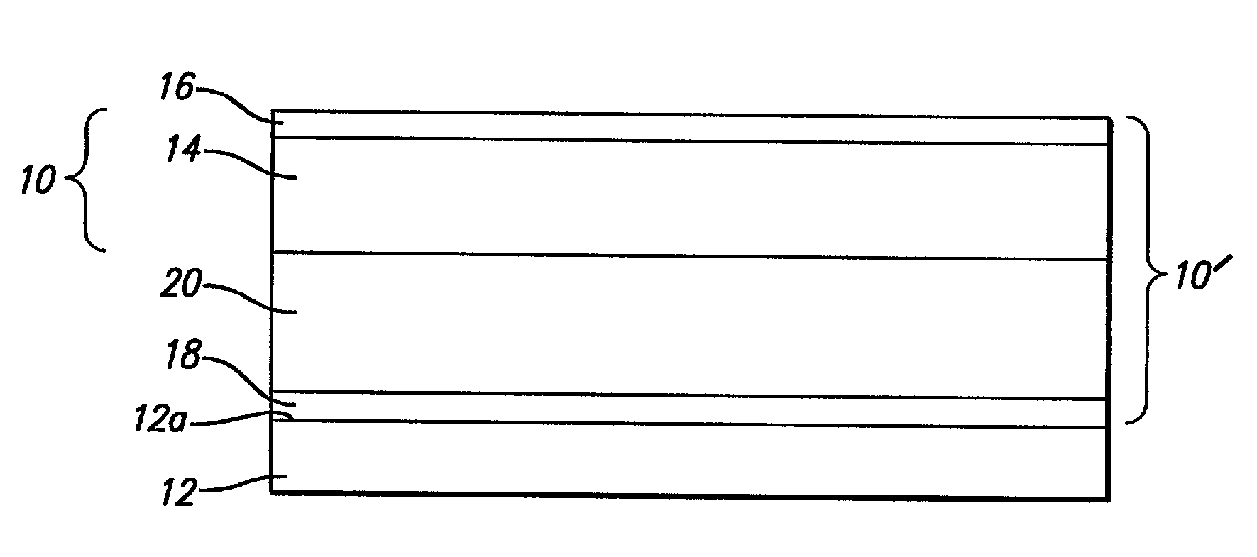
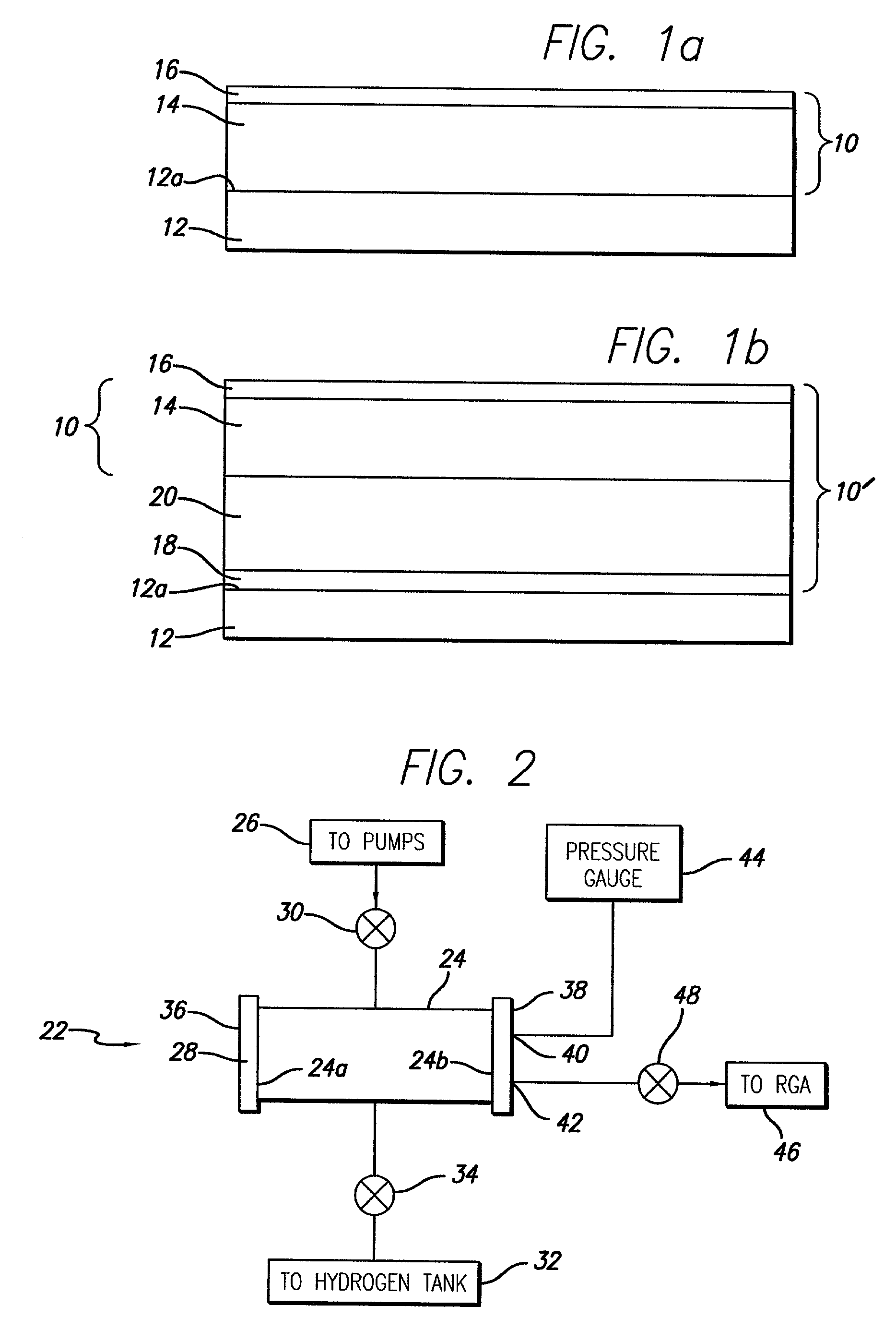
[0020] In a first embodiment, the thin film hydrogen getter 10 of the present invention consists of a vacuum-deposited multilayer film as shown in FIG. 1a, deposited on top of a surface 12a of substrate 12. A titanium (Ti) layer 14 is first vacuum-deposited, followed by a palladium (Pd) layer 16.

[0021] The titanium layer 14 has a thickness that is related to the expected generation of hydrogen over the lifetime of the package and the total area of the thin film, plus some safety margin. For example, for an expected hydrogen generation of about 75 Torr.multidot.cm.sup.3 from the package, only 0.56 mg of titanium would be required to absorb this amount of hydrogen. Factoring in a safety factor of 10, the required amount of titanium would still only be 5.6 mg.

[0022] The thickness of the palladium layer 16 must be thick enough to avoid pinholes (which would allow unwanted oxidation of the underlying titanium layer), but not so thick as to adversely affect the diffusion of hydrogen there...

second embodiment

[0030] In a second embodiment, the thin film hydrogen getter / EMI shield 10' of the present invention consists of a vacuum-deposited multilayer film as shown in FIG. 1b, deposited on top of the surface 12a of substrate 12. The EMI film comprises a thin (100 to 250 .ANG.) electrically conductive metal, for example, a Ti adhesion layer 18 followed by an aluminum 20, 100 to 200 microinch in thickness, thereby providing 5 to 6 skin depths thickness at 10 GHz. As above, the getter portion comprises the Ti layer 14, followed by the palladium Pd layer 16. Again, the titanium layer 14 has a thickness of about 40 to 80 microinch, while the palladium layer 16 has a thickness of about 8 microinch. All of the four layers 14, 16, 18, 20 are deposited during the same processing run at a vacuum of about 10.sup.-6 Torr. Alternatively, the Ti adhesion layer 18 may be omitted, and instead, a copper or nickel layer, deposited by electroless deposition, may be deposited directly on the dielectric substr...


PUM

PropertyMeasurementUnit
Thicknessaaaaaaaaaa
Molar densityaaaaaaaaaa

Abstract

A thin film hydrogen getter is provided for protecting GaAs circuitry sealed in an hermetic package. The thin film getter which comprises a multilayer metal film which is deposited by vacuum evaporation techniques onto a surface of the packaging. The multilayer film comprises (1) a titanium film and (2) palladium film which is deposited onto the titanium film. Both the titanium and the palladium are deposited during the same coating process run, thereby preventing the titanium from being oxidized. The palladium continues to prevent the titanium from being oxidized once the getter is exposed to the atmosphere. However, hydrogen is easily able to diffuse through the palladium into the titanium where it is chemically bound up, since palladium is highly permeable to hydrogen. If EMI shielding is desired, a conductive metal, such as aluminum or copper, can first be formed between the packaging and the titanium layer.

Description

[0001] The present application is related to application Serial No. ______, filed on ______ and entitled "Dielectric Interconnect Frame Incorporating EMI Shield and Hydrogen Absorber for Tile T / R Modules" [PD-00W125]. That application is directed to dielectric interconnect frames, used in GaAs hermetically-sealed packaging.[0002] The present invention relates to packaging of gallium arsenide (GaAs) integrated circuits, and, more particularly, to a hydrogen getter for chemically binding up hydrogen evolved from packaging materials.[0003] Gallium Arsenide (GaAs) integrated circuits which are hermetically packaged will suffer from reduced performance and reliability if the hydrogen that is evolved from the packaging materials is allowed to diffuse into the GaAs devices. Hydrogen concentrations as low as 500 ppm have been demonstrated to decrease the mean time to failure. A prior art solution to this problem of hydrogen poisoning is to insert a material into the package which chemically...

Claims


Application Information

Patent Timeline
IPC IPC(8): F25B9/02H01L23/26
CPCH01L23/26H01L23/552H01L2924/1423Y10S428/938Y10T428/12569H01L2924/0002Y10T428/12806Y10T428/12875H01L2924/00H01L2924/1627
Inventor KOVACS, ALAN L.PETER, MATTHEW H.KETOLA, KURT S.LINDER, JACQUES F.
Owner RAYTHEON CO
Why Eureka
Try Eureka