

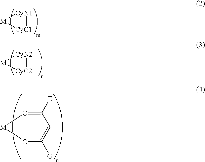
Metal coordination compound, luminescence device and display apparatus
- Summary
- Abstract
- Description
- Claims
- Application Information
AI Technical Summary
Problems solved by technology
Method used
Image

Examples
example 2
(Synthesis of Example Compound No. 43)
[0143] 13
[0144] In a 100 ml-three-necked flask, 1.18 g (4.98 mM) of 2,5-dibromopyridine, 3.57 g (15.0 mM) 2-(9,9-dimethylfluorenyl)boronic acid prepared in Example 1, 10 ml of toluene, 5 ml of ethanol and 10 ml of 2M-sodium carbonate aqueous solution were placed and stirred at room temperature under nitrogen stream, and 0.35 g (0.30 mM) of tetrakis(triphenylphosphine)-palladium (0) was added thereto. Thereafter, reflux under stirring was performed for 12 hours under nitrogen stream. After completion of the reaction, the reaction product was cooled on an ice bath to precipitate a crystal, which was then filtered out and washed with water. To the crystal, 100 ml of methanol was added and washed at room temperature under stirring, and then was recovered by filtration. The resultant crystal was purified by silica gel column chromatography (eluent: chloroform) to obtain 2.10 g (yield=91.0%) of 2,5-bis{2-(9,9-dimethyl-fluorenyl)}pyridine (colorless cr...
examples 3-11
[0147] Each of luminescence devices having a layer structure shown in FIG. 1B were prepared in the following manner.
[0148] On a 1.1 mm-thick glass substrate (transparent substrate 15), a 100 nm-thick film (transparent electrode 14) of ITO (indium tin oxide) was formed by sputtering, followed by patterning to form a stripe electrode including 100 lines each having a width of 100 nm and a spacing with an adjacent line of 10 nm (i.e., electrode pitch of 110 nm).
[0149] On the ITO-formed substrate, three organic layers and two metal electrode layers shown below were successively formed by vacuum (vapor) deposition using resistance heating in a vacuum chamber (10.sup.-4 Pa).
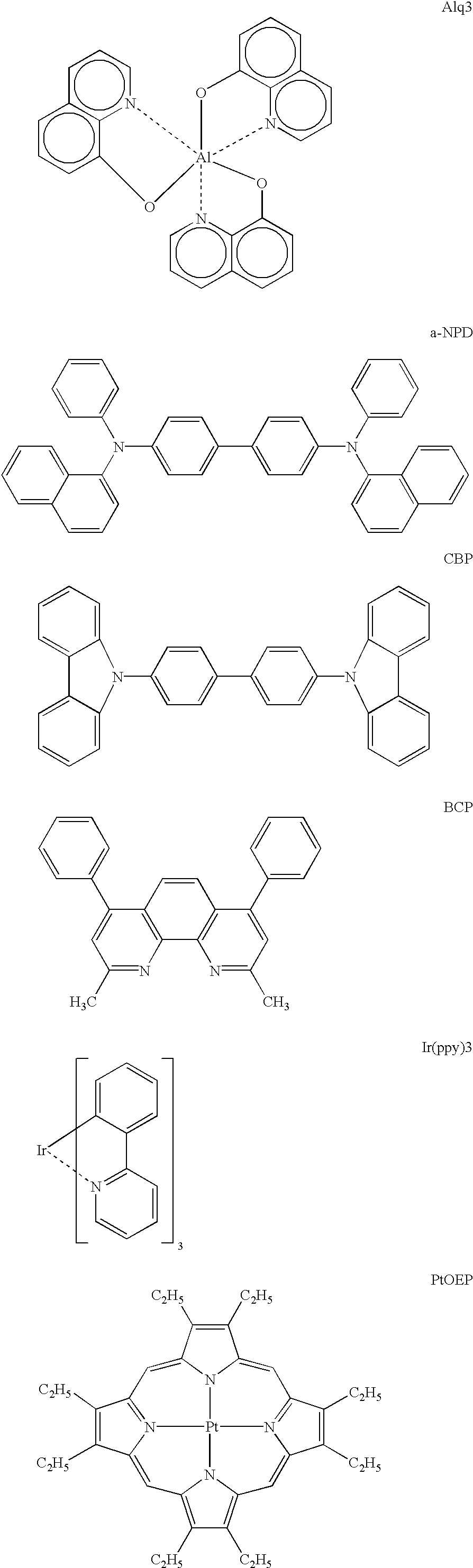
[0150] Organic layer 1 (hole transport layer 13) (40 nm): .alpha.-NPD
[0151] Organic layer 2 (luminescence layer 12) (30 nm): co-deposited film of CBP:metal complex (metal coordination compound shown in Table 45) (95:5 by weight)
[0152] Organic layer 3 (electron transport layer 16) (30 nm): Alq3
[0153] Metal electrode lay...
example 12
[0162] A color organic EL display apparatus shown in FIG. 2 was prepared in the following manner.
[0163] An active matrix substrate had a planar structure basically similar to a structure described in U.S. Pat. No. 6,114,715.
[0164] Specifically, on a 1.1 mm-thick glass substrate, top gate-type TFTs of polycrystalline silicon were formed in an ordinary manner and thereon, a flattening film was formed with contact holes for electrical connection with a pixel electrode (anode) at respective source regions, thus preparing an active matrix substrate with a TFT circuit.
[0165] On the active matrix substrate, a 700 nm-thick pixel electrode (anode) of ITO having a large work function was formed in a prescribed pattern. On the ITO electrode, prescribed organic layers and a 100 nm-thick Al electrode (cathode) were successively formed by vacuum deposition with a hard mask, followed by patterning to form a matrix of color pixels (128.times.128 pixels).
[0166] The respective organic layers correspo...
PUM
 Abstract
Description
Claims
Application Information