Vapor deposition device

a technology of vapor deposition and luminescent devices, which is applied in the direction of vacuum evaporation coating, electroluminescent light sources, coatings, etc., can solve the problems of very high manufacturing cost of luminescent devices, low efficiency of utilizing expensive el materials, and 1%

Inactive Publication Date: 2003-12-04
SEMICON ENERGY LAB CO LTD
View PDF99 Cites 124 Cited by
  • Summary
  • Abstract
  • Description
  • Claims
  • Application Information

AI Technical Summary

Benefits of technology

[0233] According to the invention, it is not necessary to rotate the board and therefore, a vapor deposition device capable of dealing with a large area board can be provided. Further, board holding means using a large area board and suitable for multiface cutting can be provided.
[0234] Further, according to the invention, a distance between a board and a vapor deposition source holder can be shortened and small-sized formation of a vapor deposition device can be achieved. Further, since the vapor deposition device is small-sized, a sublimated vapor deposition material adhering to an inner wall or an adherence preventive shield at inside of a film forming chamber can be reduced and a vapor deposition material can effectively be utilized.
[0235] Further, the invention can provide a fabricating device continuously arranged with a plurality of film forming chambers for carrying out vapor deposition processings. Since parallel processings are carried out at the plurality of film forming chambers in this way, throughput of a luminescent device is promoted.
[0236] Further, the invention can provide a fabricating system capable of installing a vessel filled with a vapor deposition material directly to a vapor deposition device without exposing to atmosphere. According to the invention, handling of a vapor deposition material is facilitated and an impurity can be avoided from mixing to the vapor deposition material. According to the fabricating system, a vessel filled with a material maker can directly be installed to a vapor deposition device and therefore, oxygen or water can be prevented from adhering to a vapor deposition material and further ultra high purity formation of a luminescent element in the future can be dealt with.

Problems solved by technology

Therefore, in forming the EL layer, an efficiency of utilizing the expensive EL material is extremely low i.e. about 1% or smaller and fabricating cost of a luminescent device becomes very expensive.
Further, the vapor deposition device is of a structure of rotating the board and therefore, there is a limit in the vapor deposition device aiming at a large area board.
Further, there is a problem that the EL material is easily oxidized due to presence of oxygen or water to be deteriorated.
However, in forming a film by a vapor deposition method, a predetermined amount of a vapor deposition material put into a vessel (glass bottle) is taken out and transferred to a vessel (representatively, crucible, or vapor deposition boat) installed at a position opposed to an object to be formed with a film at inside of a vapor deposition device and there is a concern that the vapor deposition material is mixed with oxygen or water or an impurity in the transferring operation.
However, when the glove is provided at the pretreatment chamber, the chamber cannot be subjected to vacuum, the operation is carried out under atmospheric pressure and there is a high possibility of mixing an impurity.
Even when the transferring operation is carried out at inside of the pretreatment chamber subjected to a nitrogen atmosphere, it is difficult to reduce moisture or oxygen as less as possible.
Further, although it is conceivable to use a robot, since the vapor deposition material is in a powder-like shape and therefore, it is very difficult to fabricate the robot for carrying out the transferring operation.
Therefore, it is difficult to perform steps of forming an EL element, that is, from a step of forming an EL layer above a lower electrode to a step of forming an upper electrode, by an integrated closed system preventing an impurity from mixing.
According to the above-described large area board, there is conceivable a problem that when the board is fixedly held by board holding means (permanent magnet or the like), the board is bent partially.
Further, when the larger area is formed, there is also a concern of bending a thin mask.

Method used


Image

  • Vapor deposition device
  • Vapor deposition device
  • Vapor deposition device

Examples


example 1

[0118] In this example, an example of forming TFT on a substrate having an insulating surface and forming an EL element, that is a light emitting element, is shown in FIG. 10. A cross-sectional view of one TFT that is connected to an EL element in a pixel portion is shown in this example.

[0119] A base insulating film 201 is formed by a lamination of insulating films such as a silicon oxide film, a silicon nitride film or a silicon oxynitride film on a substrate 200 having an insulating surface. Although the base insulating film 201 herein uses a two-layer structure, it may use a structure having a single layer or two layers or more of the insulating films. The first layer of the base insulating film is a silicon oxynitride film formed to have a thickness of 10 to 200 nm (preferably 50 to 100 nm) by a plasma CVD using a reaction gas of SiH.sub.4, NH.sub.3 and N.sub.2O. Herein, a silicon oxynitride film is formed (composition ratio: Si=32%, O=27%, N=24% and H=17%) having a film thickn...

embodiment 3

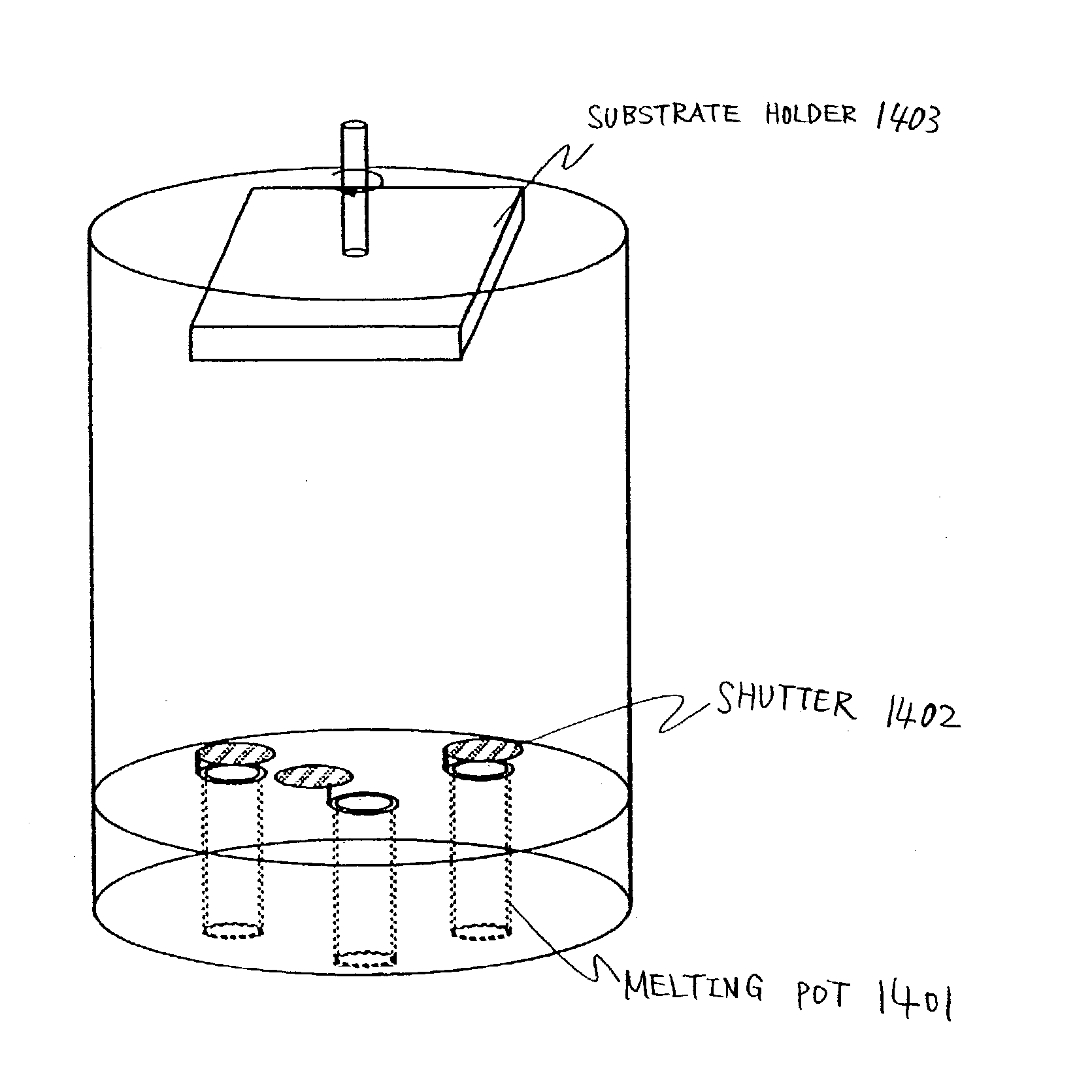
[0134] In case of using vacuum-evaporation, as shown in Embodiment 3, a container (typically, a melting pot) in which an EL material that a vacuum-evaporation material is stored in advance by a material maker is set in a deposition chamber. Preferably, the melting pot is set in the deposition chamber while avoiding contact with the air. A melting pot shipped from a material maker is preferably sealed in a second container during shipment and is introduced into a deposition chamber in that state. Desirably, a chamber having vacuum exhaust means is connected to the deposition chamber (installing chamber), the melting pot is taken out of the second container in vacuum or in an inert gas atmosphere in this chamber, and then the melting pot is set in the deposition chamber. In this way, the melting pot and the EL material stored in the melting pot are protected from contamination.

[0135] Next, a second electrode 219 is formed as a cathode on the light-emitting layer. The second electrode ...

example 2

[0153] According to the example, FIG. 12 shows an example of a fabricating device of a multichamber system fully automating fabrication of from a first electrode to sealing.

[0154] FIG. 12 shows a multichamber fabricating device having gates 10a through 100x, a preparing chamber 101, a take-out chamber 119, carrying chambers 102, 104a, 108, 114 and 118, delivery chambers 105, 107 and 111, deposition chambers 106R, 106B, 106G, 106H, 106E, 109, 110, 112 and 113, installing chambers for installing evaporation sources 126R, 126G, 126B, 126E and 126H, a pretreatment chamber 103, a sealed board loading chamber 117, a sealing chamber 116, cassette chambers 111a and 111b, a tray mounting stage 121, a cleaning chamber 122, a baking chamber 123 and a mask stock chamber 124.

[0155] A procedure of carrying a board previously provided with a thin film transistor, an anode and an insulator for covering an end portion of the anode to the fabricating device shown in FIG. 12 and fabricating a luminesc...


PUM

PropertyMeasurementUnit
heightaaaaaaaaaa
heightaaaaaaaaaa
heightaaaaaaaaaa

Abstract

The present invention provides a vapor deposition device suitable for multiface cutting by using a large area board, having a high efficiency of utilizing an EL material and excellent in uniformity of a film, wherein a board 13 and a vapor deposition mask 14 are mounted above board holding means 12, an interval between a vapor deposition source holder 17 and an object to be deposited (board 13) is narrowed to be equal to or smaller than 30 cm, preferably, equal to or smaller than 20 cm, further preferably, 5 through 15 cm and in vapor deposition, the vapor deposition source holder 17 is moved in the X direction or Y direction in accordance with an insulating member (referred to also as bank, partition wall) 10 and a shutter 15 is opened and closed to thereby form a film.

Description

[0001] The present invention relates to a deposition system for depositing materials which can be deposited by evaporation (hereinafter, an evaporation material), and a manufacturing method of a luminescent device typified by an organic light emitting element that is formed using the deposition system. Specifically, the present invention relates to a vacuum-evaporation method and an evaporation system that conducts deposition by evaporating an evaporation material from a plurality of evaporation sources provided to face a substrate.RELATED ART[0002] In recent years, research related to a luminescent device having an EL element as a self-luminous light emitting element has been activated. The luminescent device is referred to as organic EL display (OELD) or organic light emitting diode (OLED). Since these luminescent devices have characteristics such as rapid speed of response that is suitable for movie display, low voltage, low power consumption driving, or the like, they attracts a...

Claims


Application Information

Patent Timeline
Patent Type & Authority Applications(United States)
IPC IPC(8): C23C14/04H05B33/10C23C14/12C23C14/24C23C14/56H01L51/40H01L51/50H01L51/56H05B33/14
CPCC23C14/042C23C14/24C23C14/246H01L51/56H01L51/001H01L51/0013C23C14/56H10K71/18H10K71/164H10K71/00H05B33/10
Inventor YAMAZAKI, SHUNPEI
Owner SEMICON ENERGY LAB CO LTD
Why Eureka
Try Eureka