
Imaging members

a technology of electrophotography and imaging member, which is applied in the direction of corona discharge, instruments, cameras, etc., can solve the problems of increasing residual voltage, non-uniformity of images, and small molecule crystallization with increasing concentrations in the polymer binder, and achieves more expensive coating and cleaning procedures

Inactive Publication Date: 2004-04-08
XEROX CORP
View PDF9 Cites 31 Cited by
  • Summary
  • Abstract
  • Description
  • Claims
  • Application Information

AI Technical Summary

Benefits of technology

[0016] By the use of the disclosed synthesized mixture of symmetric and / or unsymmetric charge transport molecules in the charge transport layer of the present invention, a charge transport layer of an imaging member is achieved that has excellent hole transporting performance and wear resistance, and that is able to be coated onto the imaging member structure using known conventional methods.
[0030] The blocking layer is continuous and may have a thickness of less than about 10 micrometers because greater thicknesses may lead to undesirably high residual voltage. In embodiments, a blocking layer of from about 0.005 micrometers to about 1.5 micrometers facilitates charge neutralization after the exposure step and optimum electrical performance is achieved. The blocking layer may be applied by any suitable conventional technique such as spraying, dip coating, draw bar coating, gravure coating, silk screening, air knife coating, reverse roll coating, vacuum deposition, chemical treatment, and the like. For convenience in obtaining thin layers, the blocking layer is in embodiments applied in the form of a dilute solution, with the solvent being removed after deposition of the coating by conventional techniques, such as, by vacuum, heating, and the like. Generally, a weight ratio of blocking layer material and solvent of from about 0.05:100 to about 5:100 is satisfactory for spray coating.
[0034] The active charge transport layer may comprise any suitable transparent organic polymer or non-polymeric material capable of supporting the injection of photo-generated holes and electrons from the charge generating layer and allowing the transport of these holes or electrons through the organic layer to selectively discharge the surface charge. The active charge transport layer not only serves to transport holes or electrons, but also protects the photoconductive layer from abrasion or chemical attack and therefore extends the operating life of the photoreceptor imaging member. The charge transport layer should exhibit negligible, if any, discharge when exposed to a wavelength of light useful in xerography, for example, 4,000 Angstroms to 8,000 Angstroms. Therefore, the charge transport layer is substantially transparent to radiation in a region in which the photoconductor is to be used. Thus, the active charge transport layer is a substantially non-photoconductive material which supports the injection of photogenerated holes or electrons from the generating layer. The active transport layer is normally transparent when exposure is effected through the active layer to ensure that most of the incident radiation is utilized by the underlying charge generating layer for efficient photogeneration. The charge transport layer in conjunction with the generating layer is a material which is an insulator to the extent that an electrostatic charge placed on the transport layer is not conductive in the absence of illumination, that is, does not discharge at a rate sufficient to prevent the formation and retention of an electrostatic latent image thereon.
[0043] The solvent system can be included as a further component of the charge transport layer material. Conventional binder resins for charge transport layers have utilized the use of methylene chloride as a solvent to form a coating solution, for example, that renders the coating suitable for application via dip coating. However, methylene chloride has environmental concerns that usually require this solvent to have special handling and results in the need for more expensive coating and clean-up procedures. Currently, however, binder resins can be dissolved in a solvent system that is more environmentally friendly than methylene chloride, thereby enabling the charge transport layer to be formed less expensively than with some conventional polycarbonate binder resins. In embodiments, a solvent system for use with the charge transport layer material of the present invention comprises tetrahydrofuran, toluene, and the like.

Problems solved by technology

One problem encountered with photoreceptors comprising a charge generating layer and the charge transport layer is that the charge transport component consisting of small organic molecules dissolved in a polymer binder can result in the small molecule crystallizing with increasing concentrations in the polymer binder.
This crystallization can result in non-uniformity of images, increased residual voltages, and the early development of dynamic fatigue charge transport layer cracking during, for example, photoreceptor belt machine function.

Method used


Image

  • Imaging members
  • Imaging members
  • Imaging members

Examples


example ii

[0050] Three photoreceptors were prepared by forming coatings using conventional techniques on a substrate comprising vacuum deposited titanium layer on a polyethylene terephthalate film. The first coating was a siloxane barrier layer formed from hydrolyzed gamma-aminopropyltriethoxysilane having a thickness of 0.005 micrometers (50 Angstroms). The barrier layer coating composition was prepared by mixing 3-aminopropyltriethoxysilane (available from PCR Research Center Chemicals of Florida) with ethanol in a 1:50 volume ratio. The coating composition was applied by a multiple clearance film applicator to form a coating having a wet thickness of 0.5 millimeter. The coating was then allowed to dry for 5 minutes at room temperature, followed by curing for 10 minutes at 110 degrees Centigrade in a forced air oven. The second coating was an adhesive layer of polyester resin (49,000, available from E.I. duPont de Nemours & Co.) having a thickness of 0.005 micrometers (50 Angstroms). The se...


PUM


Abstract

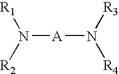
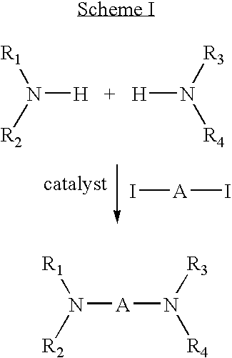
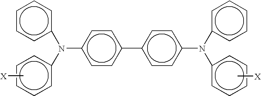
A member including for example, a substrate, a charge generating layer, a charge transport layer comprising a synthesized mixture of N,N,N',N'-Tetra-p-tolyl-biphenyl-4,4'-diamine N,N'-Diphenyl-N,N'-di-m-tolyl-biphenyl-4,4'-diamine N,N'-Bis-(4-butyl-phenyl)-N,N'-di-p-tolyl-biphenyl-4,4'-diamine N,N'-Bis-(4-butyl-phenyl)-N,N'-di-m-tolyl-biphenyl-4,4'diamine N-Phenyl-N-m-tolyl-N',N'-di-p-tolyl-biphenyl-4,4'-diamine N-(4-Butyl-phenyl)-N,N',N'-tri-p-tolyl-biphenyl-4,4'-diamine N-(4-Butyl-phenyl)-N'-phenyl-N'-m-tolyl-N-p-tolyl-biphenyl-4,4'-diamine N-(4-Butyl-phenyl)-N-m-tolyl-N',N'-di-p-tolyl-biphenyl-4,4'-diamine N-(4-Butyl-phenyl)-N'-phenyl-N,N'-di-m-tolyl-biphenyl-4,4'-diamine N,N'-Bis-(4-butyl-phenyl)-N-m-tolyl-N'-p-tolyl-biphenyl-4,4'-diamine, and a film forming binder

Description

CROSS REFERENCE TO COPENDING APPLICATION[0001] U.S. patent application Ser. No. 10 / 201,874, filed in the names of Y. Tong, et al on Jul. 23, 2002, discloses a photoconductive imaging member which is comprised of a supporting substrate, and thereover a layer comprised of a charge transport layer comprising a charge transport material containing a dendrimeric molecular structure. The entire disclosure of this Patent Application is incorporated herein by reference.[0002] The present invention is generally directed to layered imaging members, imaging apparatus, and processes thereof. More specifically, the present invention relates in general to electrophotographic imaging members and more specifically, to electrophotographic imaging members having a charge transport layer comprising mixtures of at least four different symmetric and / or unsymmetric charge transport components which are less susceptible to crystallization in polymer binders, and to processes for forming images on the memb...

Claims


Application Information

Patent Timeline
Patent Type & Authority Applications(United States)
IPC IPC(8): G03G5/06
CPCG03G5/0614G03G5/061443
Inventor TONG, YUHUAYANUS, JOHN F.FULLER, TIMOTHY J.FU, MIN-HONGPROSSER, DENNIS J.VANDUSEN, SUSAN M.
Owner XEROX CORP
Learn More