Composition for organic electroluminescene element and organic electroluminescent using the same

a technology of organic electroluminescent and organic electroluminescent, which is applied in the direction of discharge tube luminescnet screen, natural mineral layered product, perylene derivative, etc., can solve the problems of low luminance and luminescence efficiency, short life, easy deterioration of properties, etc., to improve the stability of organic el device, prevent pin holes, and improve film forming properties

Inactive Publication Date: 2004-08-05
TOYO INK SC HOLD CO LTD
View PDF10 Cites 39 Cited by
  • Summary
  • Abstract
  • Description
  • Claims
  • Application Information

AI Technical Summary

Benefits of technology

0090] When the organic layer is formed by a wet system film formation method, the materials forming the organic layer are dissolved or dispersed in an appropriate solvent such as toluene, chloroform, tetrahydrofuran, or dioxane and then formed into a film. The solvent used here can be either a single solvent or a mixed solvent. In order to improve the film forming properties, prevent pin-holes in the film, etc., an appropriate polymer or an additive can be used. Examples of such a polymer include insulating polymers such as polystyrene, polycarbonate, polyarylate, polyester, polyamide, polyurethane, polysulfone, polymethyl methacrylate, polymethyl acrylate, and cellulose, photoconductive polymers such as poly-N-vinylcarbazole and polysilane, and conductive polymers such as polythiophene and polypyrrole. Examples of the additive include an antioxidant, a UV absorbing agent, and a plasticizer. In the case of wet system film formation, since the affinity between each of the compounds is good, even a compound that on its own is highly aggregated and tends to form a nonuniform film can give a good film by mixing it with a derivative having low aggregation.
0091] In order to improve the stability of the organic EL device thus obtained to temperature, humidity, the atmosphere, etc., it is also preferable to form a protective layer on the surface of the device or coat the entire device with a silicone oil, a polymer, etc.
0092] As hereinbefore described, the organic EL device obtained using Composition X or Composition Y can emit yellow to red light, improve characteristics such as the luminescence efficiency and the maximum luminance, and has a long lifetime. This organic EL device can give a practical level of luminance with a low drive voltage, and the problem of degradation, which up till now has been serious, can be suppressed. This organic EL device can therefore preferably be used as a flat panel display of a wall-mounted television, etc. or a flat luminescent material and, furthermore, it can find application as the light source of a photocopier, a printer, etc., the light source of a liquid crystal display, an instrument, etc., a display board, a signal lamp, etc.

Problems solved by technology

Compared with inorganic EL devices, conventional organic EL devices require a high drive voltage, their luminance and luminescence efficiency are low, and their properties easily deteriorate; they have therefore not been put into practical use.
None of the conventional organic EL device luminescent materials for obtaining high intensity orange to red luminescence thus have sufficient luminance, and their lifetime is short.
On the other hand, since yellow to red luminescent materials have molecular structures that are highly planar and, furthermore are highly polar, with an electron-donating portion and an electron-withdrawing portion in the molecule so as to exhibit long wavelength fluorescence, when they are used as organic EL device luminescent materials, undesirable phenomena such as `concentration quenching` in which excited molecules of the same kind interact with each other and are deactivated without emitting light easily occur.
Attempts at improvement have been made by increasing the number of substituents, introducing a sterically bulky substituent, etc., but there is a concern that the accompanying increase in the molecular weight might degrade the solvent solubility or that there might be a deterioration in the workability, such as a deterioration in the vapor deposition properties during device fabrication.

Method used


Image

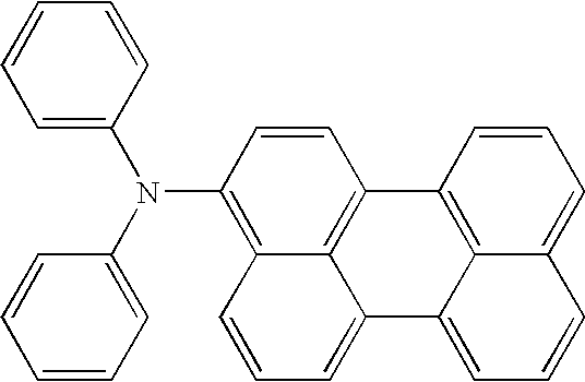
  • Composition for organic electroluminescene element and organic electroluminescent using the same
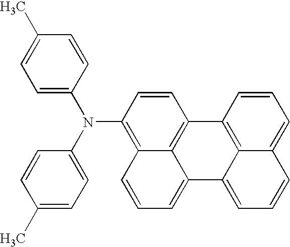
  • Composition for organic electroluminescene element and organic electroluminescent using the same
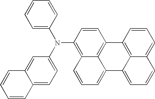
  • Composition for organic electroluminescene element and organic electroluminescent using the same

Examples


example 2

[0096] N,N'-(3-Methylphenyl)-N,N'-diphenyl-1,1'-biphenyl-4,4'-diamine (TPD) and polyvinylcarbazole (PVK) were dissolved in 1,2-dichloroethane at a ratio of 1:1, and this solution was used to form a hole injection layer at a film thickness of 50 nm on a cleaned glass plate having an ITO electrode by a spin coating method. On the top of the hole injection layer thus obtained, Compound (C1) below: 187

[0097] and Compound (B42) in Table 2 were vapor-codeposited at a ratio of 95:5 to give an electron injection type light-emitting layer having a film thickness of 60 nm. On the top thereof, a magnesium and silver alloy (mixing ratio 10:1) was vapor-deposited to form an electrode having a film thickness of 100 nm, and an organic EL device (two layer type) was thus obtained.

[0098] This device gave a red luminescence with a luminance of 1300 (cd / m.sup.2) at a dc voltage of 5 V, a maximum luminance of 18000 (cd / m.sup.2), a luminescence efficiency of 1.7 (1 m / W), and a value of x in the CIE chro...

example 3

[0100] TPD and polyvinylcarbazole (PVK) were dissolved in 1,2-dichloroethane at a ratio of 1:1, and this solution was used to form a hole injection layer at a film thickness of 50 nm on a cleaned glass plate having an ITO electrode by a spin coating method. On the top of the hole injection layer thus obtained, Compound (C2) below: 188

[0101] and DCJTB (D1) having the structure below: 189

[0102] were vapor-codeposited at a ratio of 97:3 to give an electron injection type light-emitting layer having a film thickness of 60 nm. On the top thereof, a magnesium and silver alloy (mixing ratio 10:1) was vapor-deposited to form an electrode having a film thickness of 100 nm, and an organic EL device (two layer type) was thus obtained.

[0103] This device gave a red luminescence with a luminance of 500 (cd / m.sup.2) at a dc voltage of 5 V, a maximum luminance of 9200 (cd / m.sup.2), a luminescence efficiency of 1.3 (1 m / W), and x=0.64.

[0104] The peak wavelength of the fluorescence spectrum of a soli...

example 4

[0105] Compound (A22) in Table 1 and Compound (B10) in Table 2 were dissolved in methylene chloride at a ratio of 93:7, and this solution was used to form a hole injection type light-emitting layer at a film thickness of 50 nm on a cleaned glass plate having an ITO electrode by a spin coating method. On the top of the hole injection type light-emitting layer thus obtained, bis(2-methyl-8-hydroxyquinolinate)(1-naphthalate) gallium complex was vapor-deposited to give an electron injection layer having a film thickness of 40 nm, on the top thereof a magnesium and silver alloy (mixing ratio 10:1) was vapor-deposited to form an electrode having a film thickness of 100 nm, and an organic EL device (two layer type) was thus obtained.

[0106] This device gave a red luminescence with a luminance of 2200 (cd / m.sup.2) at a dc voltage of 5 V, a maximum luminance of 15600 (cd / m.sup.2), a luminescence efficiency of 2.3 (1 m / W), and x=0.61.

[0107] The peak wavelength of the fluorescence spectrum of a...


PUM

PropertyMeasurementUnit
peak wavelengthaaaaaaaaaa
fluorescence spectrum peak wavelengthaaaaaaaaaa
wavelengthaaaaaaaaaa

Abstract

There are disclosed an organic electroluminescent (EL) device composition that includes a compound (A) having a perylene ring and a compound (B) having a diketopyrrolopyrrole skeleton, and an organic EL device that includes a pair of electrodes consisting of an anode and a cathode, and one or more organic layers including a light-emitting layer formed between the electrodes, at least one of the organic layers being a layer formed from the organic EL device composition. Furthermore, there are disclosed an organic EL device composition that includes a compound (C) having, as a solid film, a fluorescence spectrum peak wavelength of 550 nm or longer, and a compound (D) having, as a solid film in which Compound (D) is contained at 5 wt % in Compound (C), an area at a wavelength of 600 nm or shorter in a fluorescence spectrum region of 500 to 800 nm of 20% or less of the entire area, and an organic EL device including a light-emitting layer formed from this composition.

Description

[0001] The present invention relates to an organic electroluminescent (EL) device composition (material for an organic EL device) and an organic EL device employing same, the composition and device being used in flat light sources, displays, etc.[0002] The application of EL devices employing organic materials as inexpensive solid-state light-emitting, large-area full color display devices is promising, and they have been developed actively. In general, an EL device is formed from a light-emitting layer and a pair of opposing electrodes having the layer sandwiched therebetween. When an electric field is applied between the two electrodes, electrons are injected from the cathode side, and holes are injected from the anode side. When the electrons recombine with the holes in the light-emitting layer, their energy level returns from a conduction band to a valence band, and the energy is released as light. This phenomenon is called luminescence.[0003] Compared with inorganic EL devices, ...

Claims


Application Information

Patent Timeline
Patent Type & Authority Applications(United States)
IPC IPC(8): C09K11/06H01L51/00H01L51/30H01L51/50
CPCC09K11/06C09B3/14C09K2211/1007C09K2211/1011C09K2211/1014C09K2211/1029C09K2211/1033C09K2211/1037C09K2211/1044C09K2211/1088C09K2211/1092H01L51/0053H01L51/0055H01L51/0056H01L51/0058H01L51/0059H01L51/006H01L51/0061H01L51/0067H01L51/0068H01L51/0071H01L51/0072H01L51/0074H01L51/0077H01L51/0081H01L51/0089H01L51/50H01L2251/308C09B57/004C09B67/0033C09K2211/1003H10K85/623H10K85/621H10K85/624H10K85/655H10K85/631H10K85/636H10K85/626H10K85/654H10K85/633H10K85/6576H10K85/657H10K85/6572H10K85/30H10K85/351H10K85/324H10K50/00H10K2102/103
Inventor ONIKUBO, TOSHIKAZUORYU, YOSHITAKEAMANO, MASAOMIMAKI, SHINICHIROYANAI, HIROYUKIYAGI, TADAO
Owner TOYO INK SC HOLD CO LTD
Why Eureka
Try Eureka