
P-type semiconductor and semiconductor metero material and manufacturing methods thereof

a technology of metero materials and semiconductors, applied in the field of p-type semiconductors, can solve the problems of low resistance of p-type semiconductors, inability to obtain p-type nitride semiconductors with high concentration of hole carriers, and achieve low resistance, reduce the operation voltage of semiconductor devices, and reduce the effect of resistan

Inactive Publication Date: 2004-09-09
PANASONIC CORP
View PDF11 Cites 22 Cited by
  • Summary
  • Abstract
  • Description
  • Claims
  • Application Information

AI Technical Summary

Benefits of technology

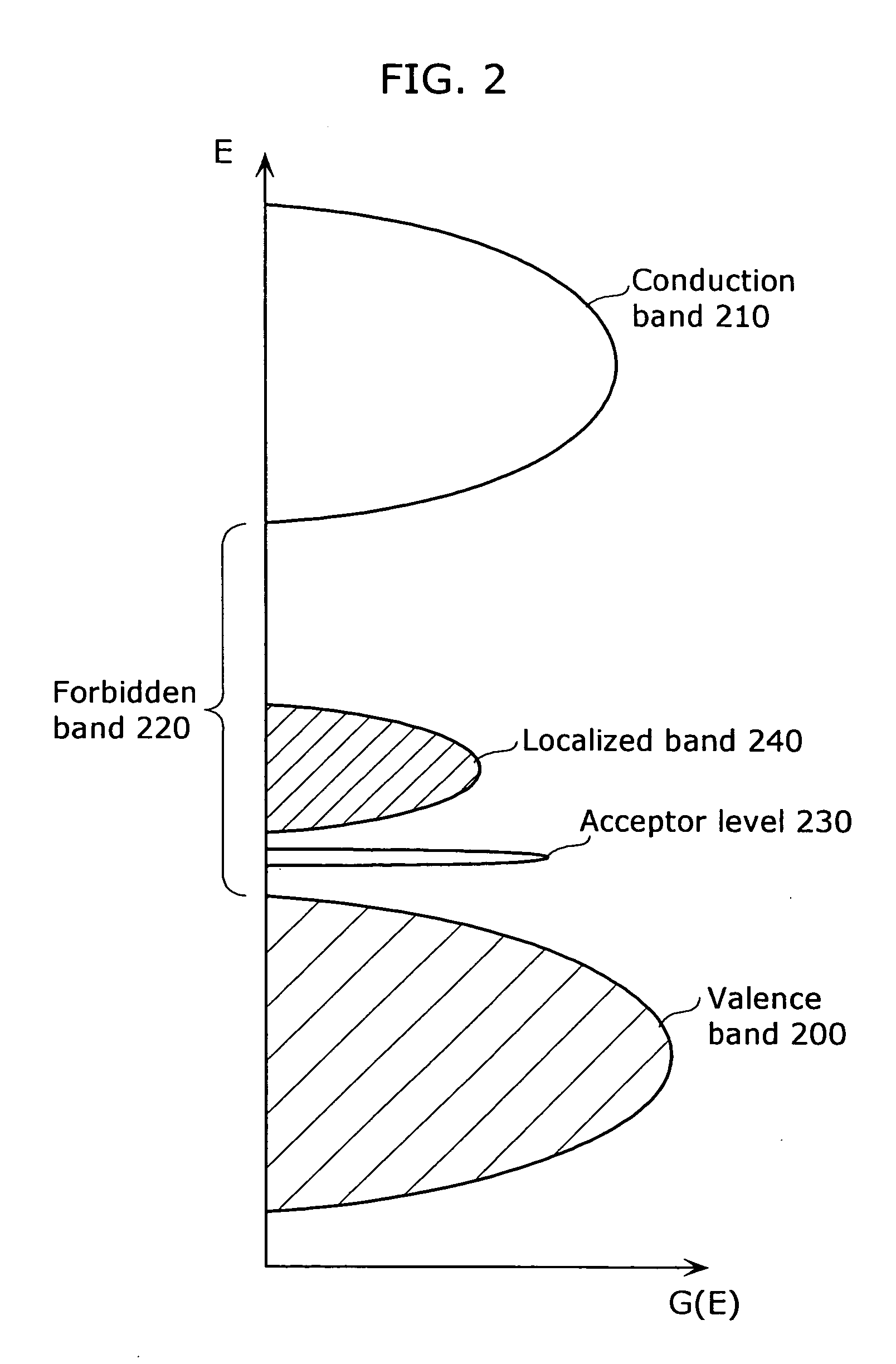
"The present invention relates to a p-type semiconductor with low resistance. The technical effect of the invention is to realize a p-type semiconductor with low resistance by using a localized band formation element that is isovalent with at least one element that composes the semiconductor and has smaller electronegativity than the element. This results in an energy band filled with electrons, which activates many holes and lowers the resistance of the p-type semiconductor. The amount of the localized band formation element is larger than the amount of the acceptor element, and the acceptor element has a lower energy level than the top of the energy band of the localized band formation element. This allows for activation of all the holes and further lowers resistance of the p-type semiconductor."

Problems solved by technology

There are some problems to realize and spread these technologies.
The biggest problem is to realize a p-type semiconductor with low resistance.
Therefore, it is impossible to obtain a p-type nitride semiconductor with high concentration of hole carriers even though an acceptor dopant is doped.
The activation energy is extremely high compared with thermal energy of about 26 meV at room temperature and therefore it is impossible to obtain a p-type gallium nitride semiconductor with high concentration of hole carriers.
Therefore, it is impossible to obtain a p-type oxide semiconductor with high concentration of hole carriers even though an acceptor dopant is doped.
The activation energy is extremely high compared with thermal energy of about 26 meV at room temperature and therefore it is impossible to obtain a p-type zinc oxide semiconductor with high concentration of hole carriers.
However, there is a problem that a p-type semiconductor with satisfactorily low resistance cannot be obtained by conventional methods for lowering resistance of a p-type semiconductor.
The activation energy is extremely high compared with thermal energy of about 26 meV at room temperature and therefore it is impossible to obtain a p-type gallium nitride semiconductor with satisfactorily low resistance.

Method used


Image

  • P-type semiconductor and semiconductor metero material and manufacturing methods thereof
  • P-type semiconductor and semiconductor metero material and manufacturing methods thereof
  • P-type semiconductor and semiconductor metero material and manufacturing methods thereof

Examples


first embodiment

[0075] (The First Embodiment)

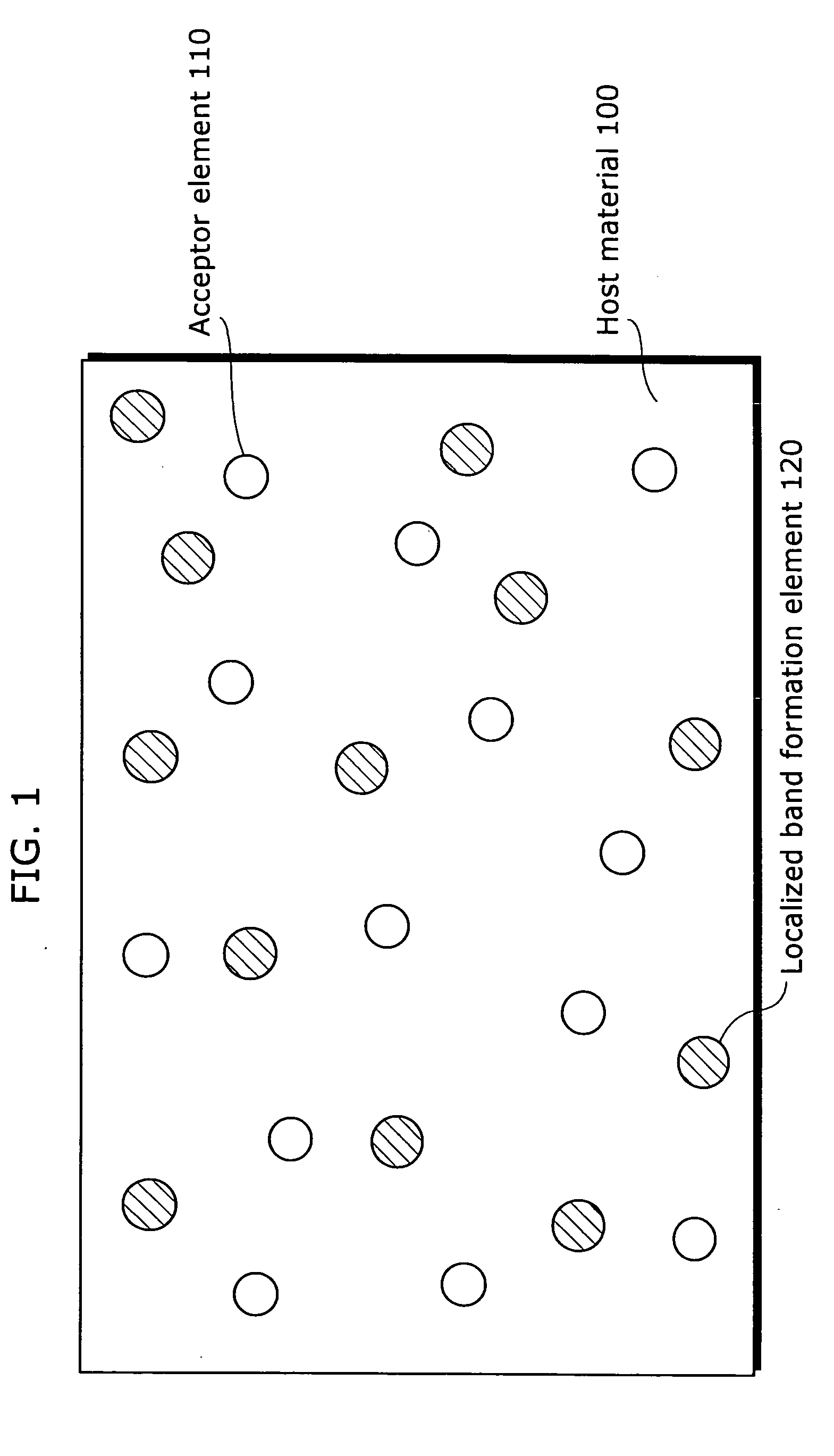
[0076] FIG. 1 is a diagram showing conceptually the structure of the p-type semiconductor according to the present embodiment.

[0077] The p-type semiconductor aims to realize a p-type semiconductor with low resistance and is composed of host material 100, an acceptor element 110 which is doped to the host material 100, and a localized band formation element 120 which is doped to the host material 100.

[0078] Here, the host material 100 is a simple semiconductor or a compound semiconductor. For example, a simple semiconductor is represented by a silicon semiconductor, a germanium semiconductor, and a diamond semiconductor; a compound semiconductor is represented by a nitride semiconductor and an oxide semiconductor. By the way, a nitride semiconductor is a compound semiconductor including at least one of the Group III elements and at least one Group V elements including nitrogen; an oxide semiconductor is a compound semiconductor including at least one of t...

first example

THE FIRST EXAMPLE

[0093] Next, a concrete example of the p-type semiconductor according to the present embodiment is shown by an example.

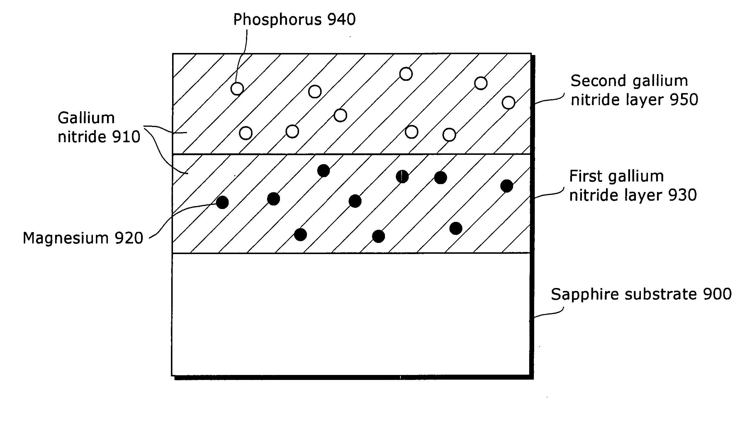
[0094] The p-type gallium nitride semiconductor according to the present example is manufactured by using trimethyl gallium (hereinafter, TMG) as the source gas of gallium, using ammonia as the source gas of nitrogen, using biscyclopentagienyl magnesium as the source gas of magnesium, using phosphine as the source gas of phosphorus, and executing epitaxial growth on a sapphire substrate by the MOCVD method. Here, the amount of phosphorus is, for example, about 2 atom %. By the way, in the present example, as a method for manufacturing the p-type gallium nitride semiconductor, the MOCVD method is exemplified. However, it is acceptable that the p-type gallium nitride semiconductor is manufactured by the MBE method, using metal gallium, metal magnesium, indium phosphide and nitrogen source generated by plasma.

[0095] FIG. 3 is a diagram showing a cross ...

second embodiment

[0103] (The Second Embodiment)

[0104] In host material 100 of the p-type semiconductor according to the first embodiment, acceptor element 110 and localized band formation element 120 are doped uniformly. However, even if the part including the acceptor element 110 and the part including the localized band formation element 120 are separated spatially, the same effect in the case of being not separated spatially is obtained. Further, in this case, since it is possible to separate spatially the part transmitting the holes and the part generating the holes and restrain the dispersion of the holes, it is possible to realize the p-type semiconductor with further low resistance. Therefore, in the p-type semiconductor according to the second embodiment, the host material including the acceptor element 110 and the host material including the localized band formation element 120 are separated spatially. Hereinafter, the different points from the first embodiments are mainly explained.

[0105] ...


PUM

PropertyMeasurementUnit
band gapaaaaaaaaaa
thermal energyaaaaaaaaaa
depthaaaaaaaaaa

Abstract

A p-type semiconductor includes a host material 100 which is a semiconductor, an acceptor element 110 and a localized band formation element 120. Here, the acceptor element 110 is doped to the host material 100 and has fewer valence electrons than valance electrons of at least one of the elements which compose the host material 100; the localized band formation element 120 is doped to the host material 100, is isovalent with at least one of the elements which compose the host material 100 and has smaller electronegativity than the electronegativity of the element(s), and forms the localized band which activates holes of an acceptor level.

Description

[0001] (1) Field of the Invention[0002] The present invention relates to a p-type semiconductor and particularly to a p-type semiconductor with low resistance.[0003] (2) Description of the Related Art[0004] In recent years, a nitride semiconductor based on gallium nitride has been commercially utilized for a full color display, a blue (long wave ranged from ultraviolet to yellow) light-emitting diode used for a signal light and the like, a write / read apparatus for optical recording media and blue laser used for a laser microscope and the like. Further, the nitride semiconductor is expected to be applied to media which enables high-density record and white light source which uses no mercury. Additionally, since an oxide semiconductor based on zinc oxide has a band gap of 3.37 eV at room temperature, resistance to reducing gas, stability at a high temperature, and excellent transparence, it is expected to be applied to a transparent conductive film and like besides the above-mentioned...

Claims


Application Information

Patent Timeline
Patent Type & Authority Applications(United States)
IPC IPC(8): H01L29/20H01L29/207
CPCH01L29/207H01L29/2003
Inventor TAKIZAWA, TOSHIYUKI
Owner PANASONIC CORP
Learn More