Light emitting element structure using nitride bulk single crystal layer

a light emitting element and single crystal layer technology, applied in the direction of crystal growth process, monocrystalline material growth, semiconductor lasers, etc., can solve the problems of red shift of light emitting, recombination degradation and increase of threshold current, and the limitation of laser device layers by vapor phase growth, etc., to achieve low or same solubility, easy to clear, and high solubility

Inactive Publication Date: 2004-12-16
AMMONO SP Z O O (PL) +1
View PDF99 Cites 193 Cited by
  • Summary
  • Abstract
  • Description
  • Claims
  • Application Information

AI Technical Summary

Benefits of technology

[0015] According to a first aspect of the present invention, there is provided a light emitting device structure comprising a gallium-containing nitride single crystal substrate, and an n-type gallium-containing nitride semiconductor layer or layers, a gallium-containing nitride semiconductor active layer and a p-type gallium-containing nitride semiconductor layer or layers by a vapor phase growth on the substrate, wherein the single crystal substrate is obtained from a gallium-containing nitride bulk single crystal, and provided with an epitaxial growth face with dislocation density of 10.sup.5 / cm.sup.2 or less. The crystal dislocation of the epitaxial growth face of the substrate according to the present invention can be reduced compared with those obtained by the so-far vapor phase growth, especially ELOG method, due to which the epitaxial layer formed thereon has a good crystalline quality without formation of a lower temperature buffer layer and the excellent device structure can be formed.
[0073] The bulk single crystal substrate according to the present invention can be used as an intermediate layer instead of the modulation doped layer 203 and the superlattice layer 204, while the n-type contact layer 202 is formed on one bottom side, and the active layer 205, p-type clad layer 206, undoped AlGaN layer 207 and p-type contact layer 208 are successively deposited on top surface so that the similar layer structure can be formed. As described above, AMMONO method which enables to form the single crystal at a low temperature allows forming an intermediate layer with less crystal dislocation and simplifying the device structure.

Problems solved by technology

Moreover, a nitride crystal is formed on C-plane as an epitaxial growth face on the heterogeneous substrate such as the SiC substrate or the sapphire substrate by a vapor phase growth, which leads the active layer of the laser structure formed thereon to have a spontaneous polarization or piezo polarization causing a deterioration of the performance such as red shift of light emitting, recombination degradation and increase of the threshold current.
To summarize the above, there is a limitation to form layers of the laser device by a vapor phase growth.
Moreover, regarding the light emitting diode, in case that the higher luminance and higher output are required, the crystal dislocation of the substrate and the intermediate layer will be a serious problem.

Method used


Image

  • Light emitting element structure using nitride bulk single crystal layer
  • Light emitting element structure using nitride bulk single crystal layer
  • Light emitting element structure using nitride bulk single crystal layer

Examples


example 2

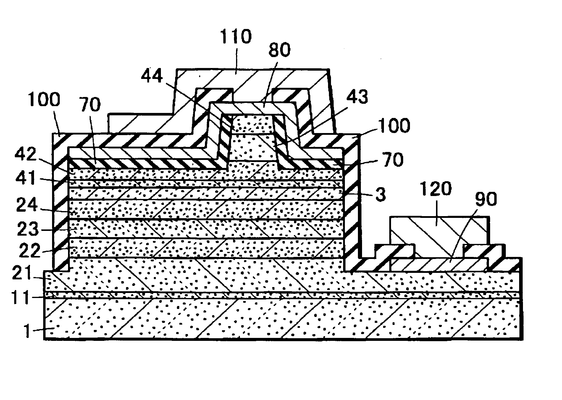
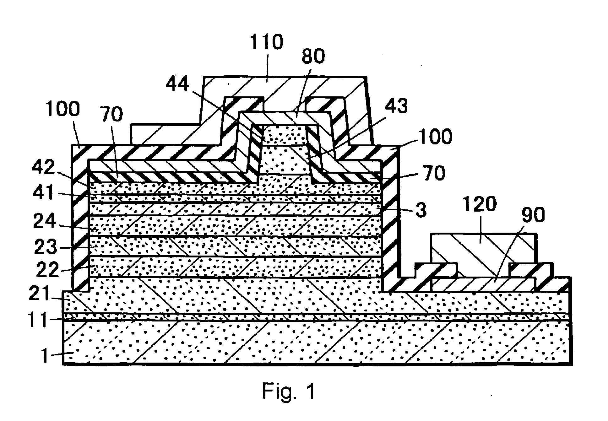
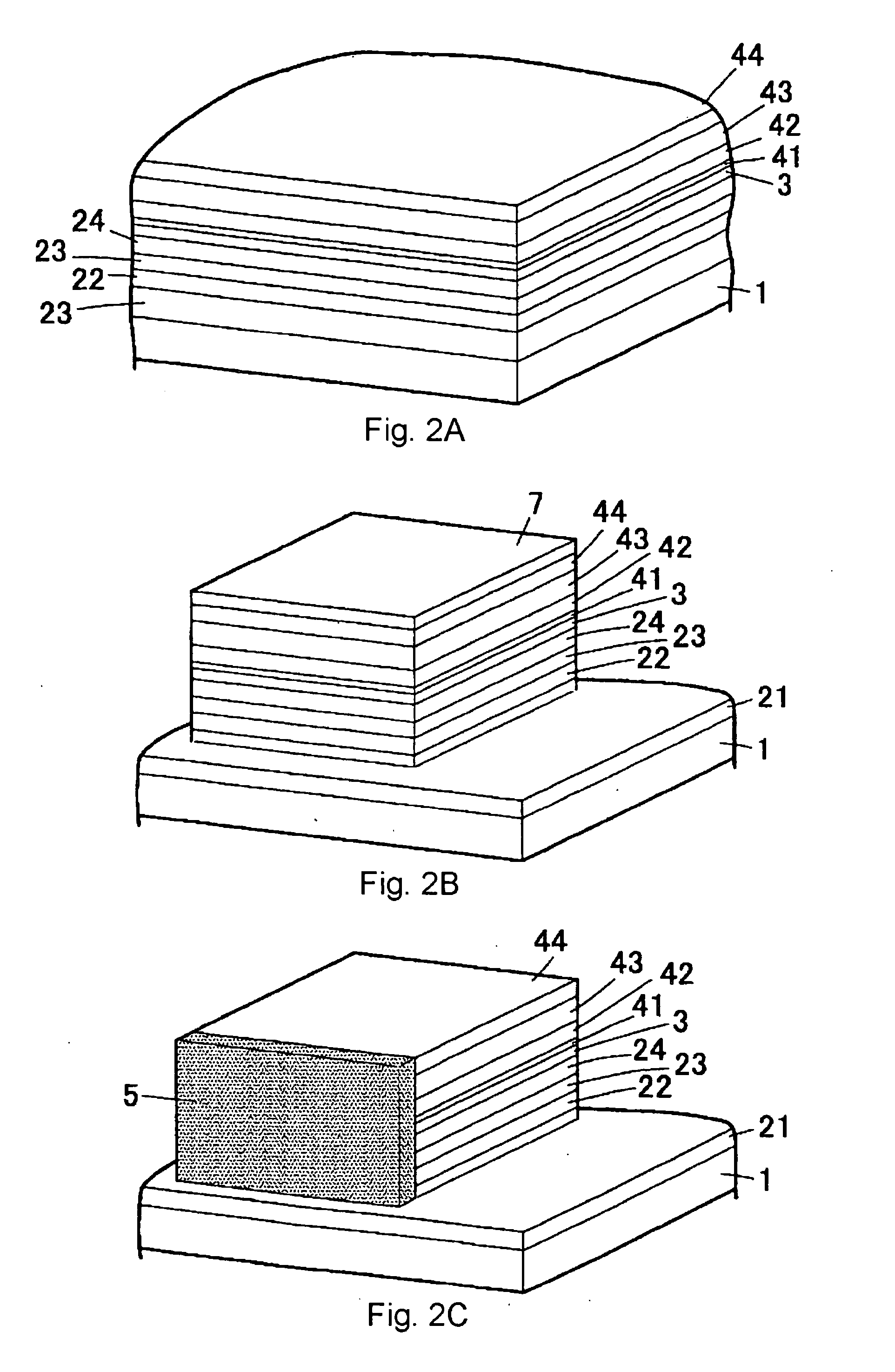
[0095] A single crystal GaN end face film of 1 .mu.m thickness is grown on the only one light emitting end face on the stripe part, whereas other stages of production of the nitride semiconductor laser device are carried out similarly as in Example 1.

[0096] Each laser device manufactured in this way is equipped with a heat sink and the laser oscillation is carried out. Prolonged laser lifetime in continuous oscillation mode is expected--with threshold current density: 2.0 kA / cm.sup.2, power output: 100 mW and 405 nm oscillation wavelength--similar as in Example 1.

example 3

[0097] A SiO.sub.2 protective film in the form of lattice pattern is deposited on the surface of the top p-type contact layer. Next, etching of RIE method is carried out so as to uncover an end face of a resonator and the surface of the n-type contact layer. Under the condition of the SiO.sub.2 mask of 0.5 .mu.m thickness formed on the surface of the p-type contact layer, the wafer is introduced into the reactor (autoclave) inside which is filled with a supercritical ammonia. In other respects, production of the nitride semiconductor laser device is carried out similarly as in Example 1.

[0098] Each laser device manufactured in this way is equipped with a heat sink and laser oscillation is carried out. Prolonged laser lifetime in continuous oscillation mode is expected--with threshold current density: 2.0 kA / cm.sup.2, power output: 100 mW and 405 nm oscillation wavelength--similarly as in Example 1.

[0099] Industrial Applicability

[0100] As described above, a bulk single crystal substr...


PUM

PropertyMeasurementUnit
temperatureaaaaaaaaaa
areaaaaaaaaaaa
widthaaaaaaaaaa

Abstract

The object of this invention is to provide a high-output type nitride light emitting device. The nitride light emitting device comprises an n-type nitride semiconductor layer or layers, a p-type nitride semiconductor layer or layers and an active layer therebetween, wherein a gallium-containing nitride substrate is obtained from a gallium-containing nitride bulk single crystal, provided with an epitaxial growth face with dislocation density of 10<5> / cm<2 >or less, and A-plane or M-plane which is parallel to C-axis of hexagonal structure for an epitaxial face, wherein the n-type semiconductor layer or layers are formed directly on the A-plane or M-plane. In case that the active layer comprises a nitride semiconductor containing In, an end face film of single crystal AlxGa1-xN (0<=x<=1) can be formed at a low temperature not causing damage to the active layer.

Description

[0001] This invention relates to a structure wherein a single crystal nitride layer prepared by a supercritical ammonia is used as a substrate or an intermediate layer of light emitting devices such as a laser structure etc.[0002] In the laser structure, crystal defect or dislocation of a waveguide causes electron-hole pairs to make non-radiative recombination therein. Ideally, considering the laser function, the dislocation density in the waveguide should be 10.sup.4 / cm.sup.2 or less. However, in the present situation, the dislocation density can not be reduced less than 10.sup.6 / cm.sup.2 by using a vapor phase epitaxial growth (MOCVD and HVPE) or by using a repeated ELOG (Epitaxial lateral overgrowth) because the waveguide is grown on a heterogeneous substrate, such as sapphire substrate or SiC substrate.[0003] The thickness of the epitaxial layer should be 100 .mu.or less to form the epitaxial layer on a sapphire substrate or a SiC layer without crack by the vapor phase growth. M...

Claims


Application Information

Patent Timeline
Patent Type & Authority Applications(United States)
IPC IPC(8): C30B7/00C30B7/10C30B9/00C30B29/40H01L21/318H01S5/00H01S5/02H01S5/028H01S5/16H01S5/22H01S5/32H01S5/323H01S5/343
CPCB82Y20/00C30B7/005C30B9/00C30B29/403C30B29/406H01S5/021H01S5/0213H01S5/0218H01S5/0281H01S5/164H01S5/22H01S5/3202H01S5/32341H01S5/34333H01S2304/12C30B7/10H01S5/32025H01S5/30
Inventor DWILINSKI, ROBERTDORADZINSKI, ROMANGARCZYNSKI, JERZYSIERZPUTOWSKI, LESZEKKANBARA, YASUO
Owner AMMONO SP Z O O (PL)
Why Eureka
Try Eureka