

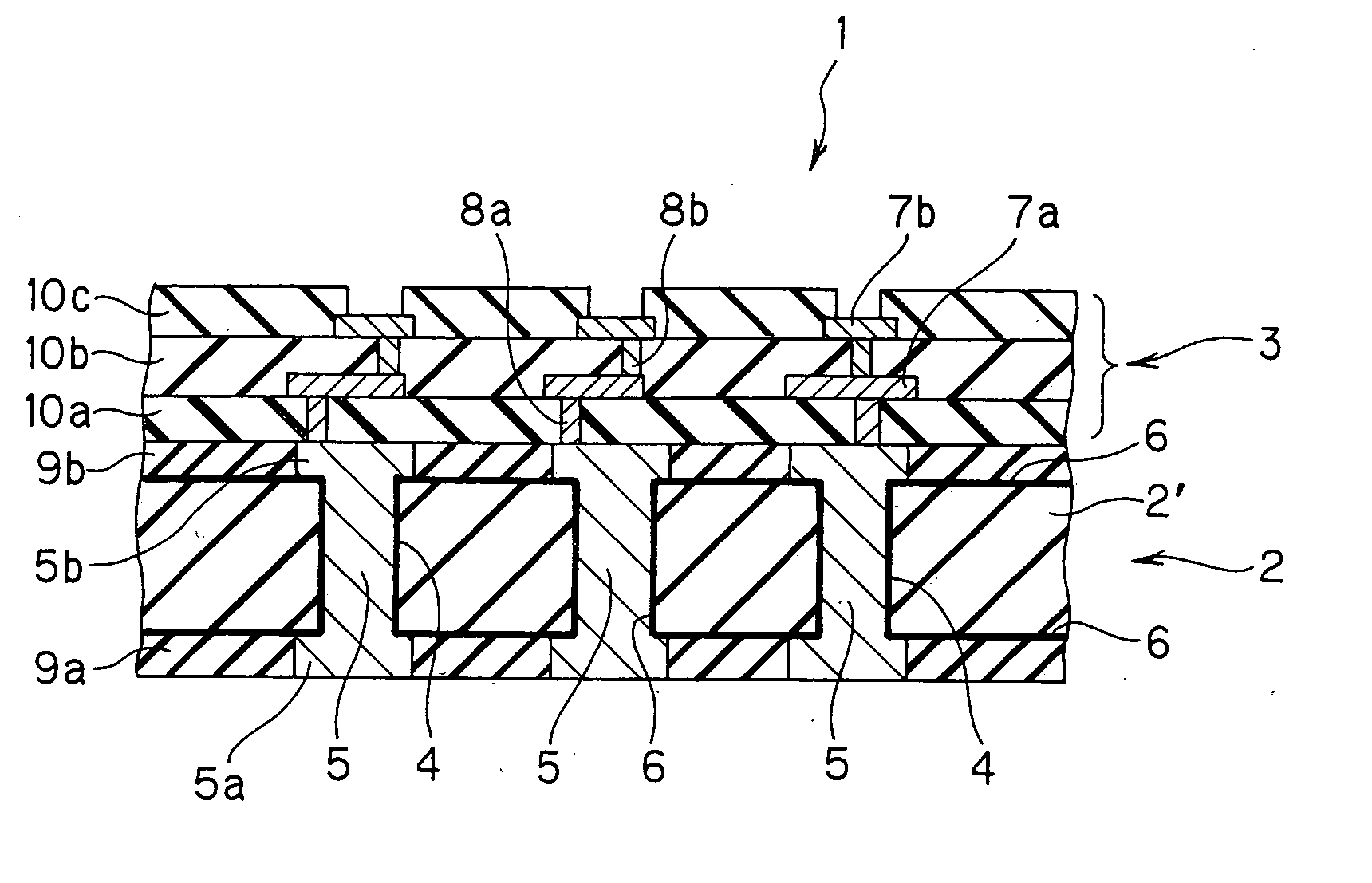
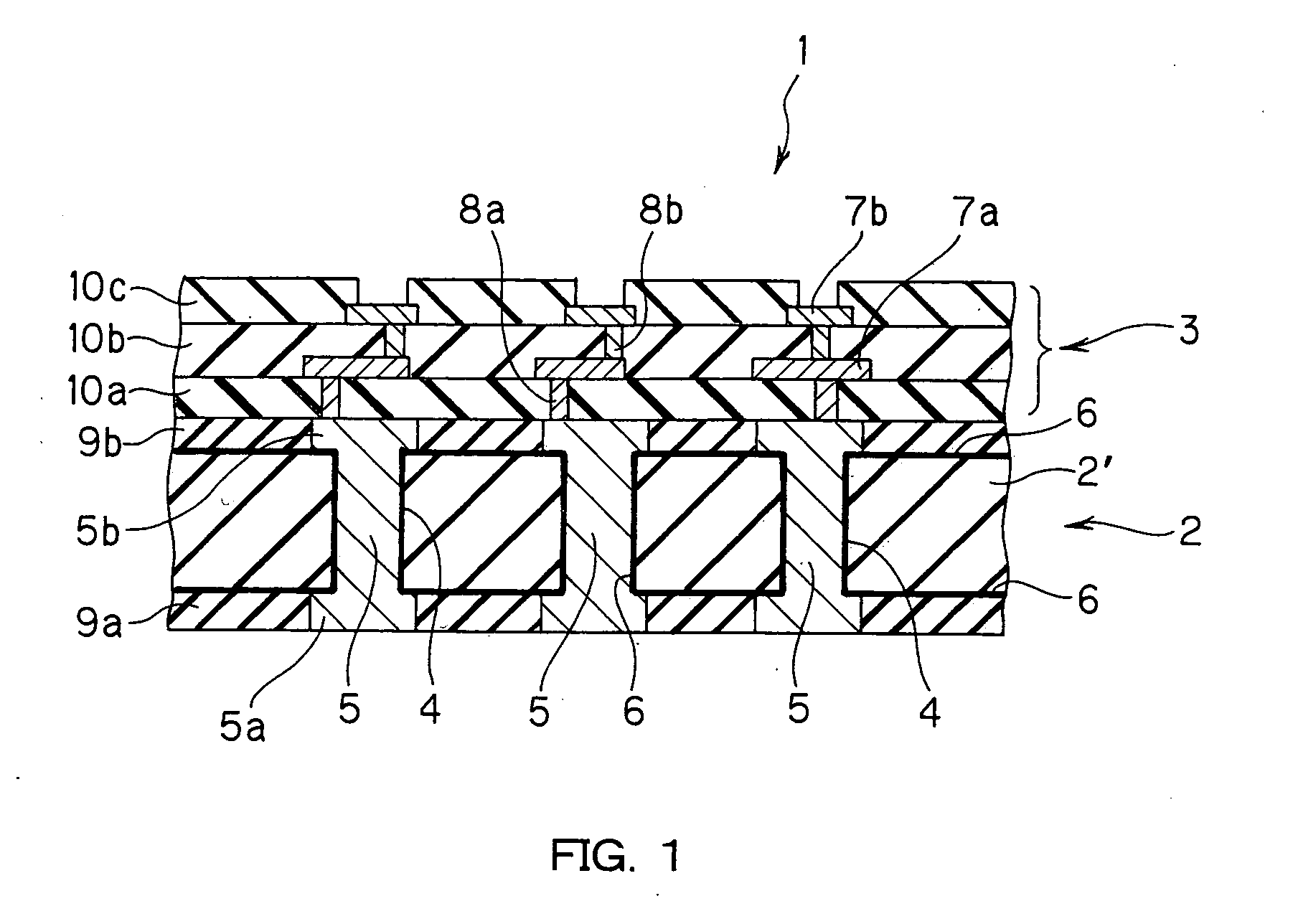
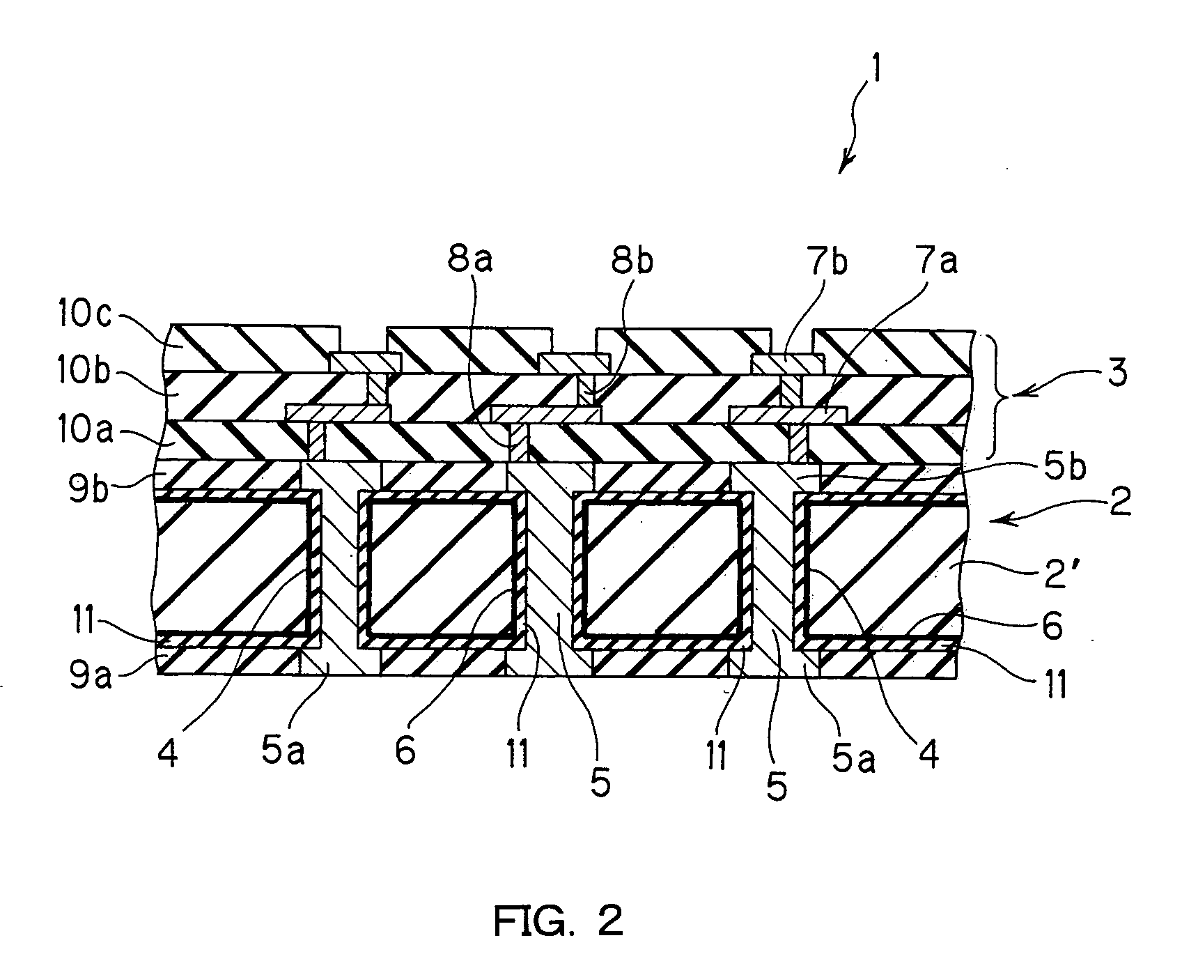
Multilayer wiring board and manufacture method thereof
a wiring board and multi-layer technology, applied in the direction of printed capacitor incorporation, insulating substrate metal adhesion improvement, printed element electric connection formation, etc., can solve the problems of limiting the degree of freedom of wiring design, raised reliability problems, and the multi-layer wiring board formed with the wiring layers on the known conventional core board by the conventional process cannot meet the demands of dimensional minimization of required electrical properties and high density wiring. , to achieve the effect of excellent electrical properties
- Summary
- Abstract
- Description
- Claims
- Application Information
AI Technical Summary
Benefits of technology
Problems solved by technology
Method used
Image

Examples
first embodiment
OF MANUFACTURE METHOD
[0134] Based on FIGS. 12A to 12E and FIGS. 13A to 13E, the first embodiment of the manufacture method of the present invention will be described.
[0135]FIGS. 12A to 12E and FIGS. 13A to 13E illustrate the manufacture method suitable for the case where silicon is used for the core member, wherein the through holes are formed by the ICP-RIE method. First, as shown in FIG. 12A, a predetermined mask pattern 31 is formed on one surface of a core member 22′ using a mask material.
[0136] Then, using the mask pattern 31 as a mask, fine holes 24′ are formed in the core member 22′ to a predetermined depth by the ICP-RIE method (FIG. 12B). As a mask material upon etching, a positive type photoresist using normal novolak resin having dry etching resistance may be used, or a silicon thin film made of silicon oxide, silicon nitride, or the like that can take a large etching selective ratio relative to silicon, or a metal thin film made of titanium, tungsten, aluminum, or the ...
second embodiment
OF MANUFACTURE METHOD
[0159]FIGS. 15A to 15E and FIGS. 16A to 16D illustrate the case wherein through holes are formed by the sandblasting method, wherein a predetermined mask pattern 51 is formed on one surface of a core member 42′ for a core board (FIG. 15A), and fine holes 44′ each having a predetermined size are formed in the core member 42′ by sandblasting using the mask pattern 51 as a mask (15B). In the present invention, the holes are not formed into penetrating holes, and the sandblasting is stopped in the stage where the perforation reaches a predetermined depth.
[0160] Then, the other surface of the core member is polished to expose the fine holes 44′ to thereby obtain through holes 44, and further obtain a desired thickness of the core member (FIG. 15C). Polishing of the core member can be implemented by a polishing machine or the like. In case of the sandblasting, since the through holes are each tapered, it is possible, by polishing to a predetermined thickness, to expo...
third embodiment
OF MANUFACTURE METHOD
[0180]FIGS. 17A to 17E and FIGS. 18A to 18B are process diagrams showing another embodiment of the multilayer wiring board manufacture method of the present invention, wherein the ICP-RIE method and the sandblasting method are jointly used.
[0181] In the multilayer wiring board manufacture method, a core member for a core board is first polished on both surfaces thereof to have a predetermined thickness, thereafter, a mask pattern 71 with a predetermined pattern is formed on one surface of the core member 62′ having the predetermined thickness (FIG. 17A). The core member can use the same material as the foregoing 22′ and 42′. Polishing of the core member can be carried out by backgrind, polishing, or the like, and a thickness of the core member 62′ after the polishing can be set taking into consideration a thickness of the core board to be produced.
[0182] Then, using the mask pattern 71 as a mask, fine holes 64′ are formed in the core member 62′ to a predetermi...
PUM
| Property | Measurement | Unit |
|---|---|---|
| thickness | aaaaa | aaaaa |
| diameter | aaaaa | aaaaa |
| diameter | aaaaa | aaaaa |
Abstract
Description
Claims
Application Information