Group-III-element nitride crystal semiconductor device

a nitride crystal, semiconductor technology, applied in the direction of semiconductor lasers, ceramic layered products, transportation and packaging, etc., can solve the problems of reducing the dislocation density, affecting the performance of the device, so as to achieve the effect of reducing the diffusion coefficien

Inactive Publication Date: 2005-04-21
PANASONIC CORP
View PDF14 Cites 53 Cited by
  • Summary
  • Abstract
  • Description
  • Claims
  • Application Information

AI Technical Summary

Benefits of technology

[0010] Hence, with such situations in mind, the present invention is intended to provide a technique for preventing impurities from diffusing in a semiconductor device produced using a substrate that is obtained by growing Group-III-element nitride crystals in a flux that is at least one of alkali metal and alkaline-earth metal.
[0012] In the semiconductor device of the present invention, since the thin film layer is formed on the Group-III-element nitride crystal substrate and has a lower diffusion coefficient than that of the substrate with respect to impurities contained in the substrate, the impurities contained in the substrate can be prevented from diffusing into the Group-III-element nitride crystal layer.

Problems solved by technology

The reduction in dislocation density therefore has been an important issue.
This method, however, includes complicated processes.
In the LPE method by which nitride crystals are grown using at least one of alkali metal and alkaline-earth metal as a flux, however, the introduction of impurities is a problem since it may change, for instance, the carrier density.
In addition, the alkali metal and alkaline-earth metal to be used as a flux are elements that are particularly susceptible to the introduction of impurities in the semiconductor processes.

Method used


Image

  • Group-III-element nitride crystal semiconductor device
  • Group-III-element nitride crystal semiconductor device
  • Group-III-element nitride crystal semiconductor device

Examples


example 1

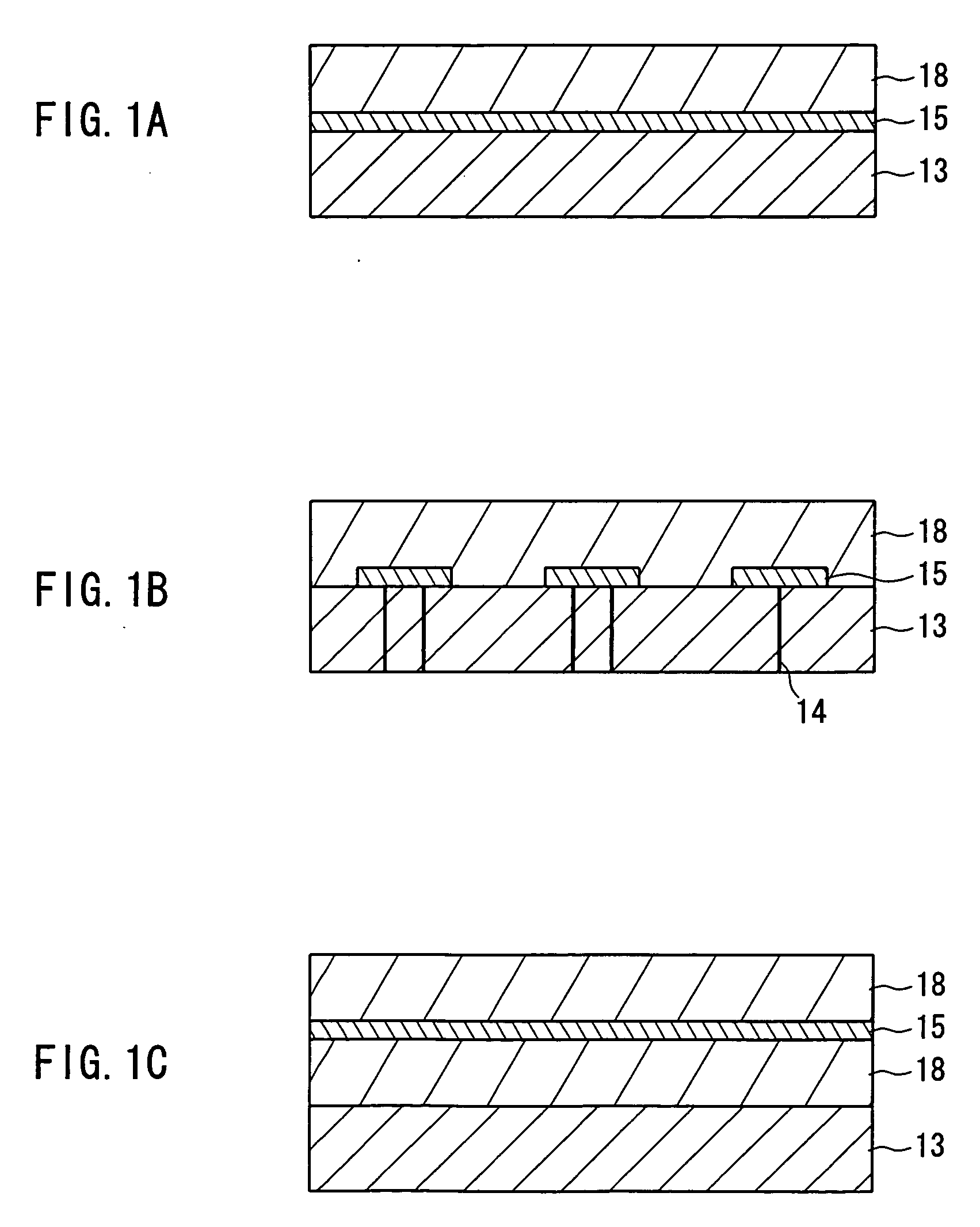
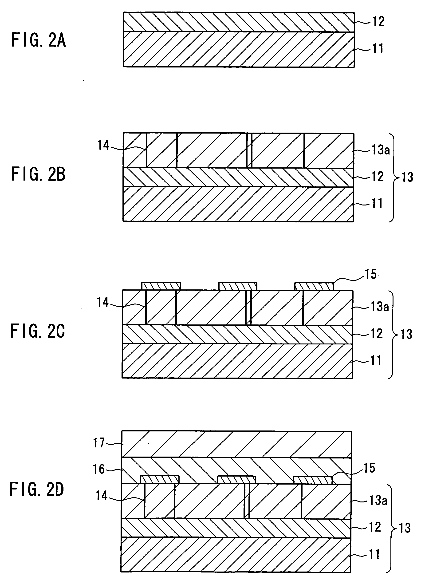
[0048] Example 1 is directed to an example of producing a semiconductor device using Group-III-element nitride crystals that are grown by the liquid phase epitaxy method on a seed layer formed selectively.

[0049] First, as shown in FIG. 3A, a support substrate 21 made of sapphire is heated to a temperature of about 1020° C. to 1100° C. and then trimethylgallium (TMG) and NH3 are supplied onto the substrate. Thus, a GaN semiconductor seed layer 22 is formed.

[0050] Next, a resist pattern is formed on the surface of the semiconductor seed layer 22 by photolithography. Subsequently, as shown in FIG. 3B, the semiconductor seed layer 22 is patterned by dry etching using Cl2 gas. The dry etching can be carried out using a reactive dry etching (RIE) apparatus of an inductive coupling type.

[0051] Subsequently, the resist pattern is removed and thus the semiconductor seed layer 22 is patterned. In addition, masks may be formed on the side faces of the semiconductor seed layer 22 and the sur...

example 2

[0066] An example of the configuration of a semiconductor laser is shown in FIG. 6. As shown in FIG. 6, first, a contact layer 52 of n-type GaN doped with Si to have a carrier density of 5×1018 cm−3 or lower was formed on a GaN substrate 51 having a thin film layer (not shown in FIG. 6). In GaN-based crystals (crystals containing Ga and N), when Si is added thereto as an impurity, holes present in Ga increase in number. Since the holes present in Ga diffuse easily, they have harmful effects in terms of, for example, lifetime when a device is formed thereon. Hence, the doping amount may be controlled so that the contact layer has a carrier density of 1×1019 cm−3 or lower, preferably 3×1018 cm−3 or lower.

[0067] Next, a cladding layer 53 of n-type Al0.07Ga0.93N and a light guiding layer 54 of n-type GaN were formed sequentially on the contact layer 52. Subsequently, a multiple quantum well (MQW) composed of a well layer (with a thickness of about 3 nm) made of Ga0.8In0.2N and a barrie...

example 3

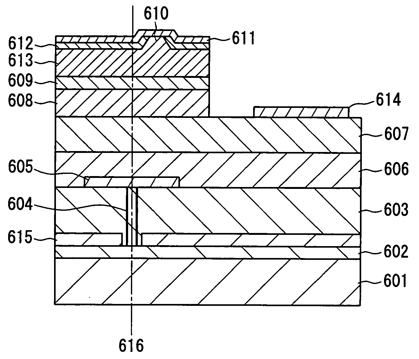
[0070] Another configuration of the semiconductor laser is shown in FIG. 7. In FIG. 7, numeral 601 indicates a support substrate, numeral 602 a seed layer, numeral 603 an LPE-GaN layer, numeral 604 threading dislocations, numeral 605 a thin film layer, numeral 606 a GaN layer, numeral 607 an n-type GaN layer, numeral 608 an n-type cladding layer, numeral 609 an active layer, numeral 610 a ridge part, numeral 611 a p-side electrode, numeral 612 an insulating film, numeral 614 an n-side electrode, numeral 615 a selective growth film, and numeral 616 a symmetry axis. As shown in FIG. 7, the ridge region 610 to serve as a laser oscillation part is located above the thin film layer 605 but is formed so as not to align with the symmetry axis 616 of the thin film layer 605. The epitaxial film (i.e. the GaN layer 606), which grows from a vapor phase on the thin film layer 605, grows from the regions where the thin film layer 605 is not located thereon and portions of the epitaxial film grow...


PUM

PropertyMeasurementUnit
thicknessaaaaaaaaaa
thicknessaaaaaaaaaa
melting pointaaaaaaaaaa

Abstract

In a Group-III-element nitride semiconductor device including a Group-III-element nitride crystal layer stacked on a Group-III-element nitride crystal substrate, the substrate is produced by allowing nitrogen of nitrogen-containing gas and a Group III element to react with each other to crystallize in a melt (a flux) containing at least one of alkali metal and alkaline-earth metal, and a thin film layer is formed on the substrate and the thin film has a lower diffusion coefficient than that of the substrate with respect to impurities contained in the substrate. The present invention provides a semiconductor device in which alkali metal is prevented from diffusing.

Description

BACKGROUND OF THE INVENTION [0001] 1. Field of the Invention [0002] The present invention relates generally to a Group-III-element nitride crystal semiconductor device. [0003] 2. Related Background Art [0004] A Group-III-element nitride compound semiconductor such as, for instance, gallium nitride (GaN) (hereinafter also referred to as a “Group-III-element nitride semiconductor” or a “GaN-based semiconductor”) has been gaining attention as a material for semiconductor elements that emit green, blue or ultraviolet light. A laser diode (LD) that emits blue light is used for high-density optical disk devices or displays while a light emitting diode (LED) that emits blue light is used for displays, lighting, etc. It is expected to use an ultraviolet LD in the field of, for instance, biotechnology and an ultraviolet LED as, for example, an ultraviolet source for a fluorescent lamp. [0005] Usually, substrates made of a Group-III-element nitride semiconductor (for instance, GaN) that are u...

Claims


Application Information

Patent Timeline
Patent Type & Authority Applications(United States)
IPC IPC(8): H01L21/20H01L21/205H01L21/208H01L21/335H01L29/15H01L29/20H01L33/02H01L33/32H01S5/00
CPCH01L21/0237H01L21/02389H01L21/02458H01L21/02521H01L21/0254H01L21/02573Y10T428/24926H01L29/155H01L29/2003H01L29/66462H01L33/02H01L33/32Y10S438/94H01L21/02625
Inventor KITAOKA, YASUOMINEMOTO, HISASHIKIDOGUCHI, ISAOTSUKAMOTO, KAZUYOSHI
Owner PANASONIC CORP
Why Eureka
Try Eureka