III-V group nitride system semiconductor substrate

Active Publication Date: 2005-05-05
SUMITOMO CHEM CO LTD
View PDF8 Cites 25 Cited by
  • Summary
  • Abstract
  • Description
  • Claims
  • Application Information

AI Technical Summary

Benefits of technology

[0046] With III-V group nitride system semiconductor substrate of this invention, even when there is a variation in inclination of crystal axis as a problem specific to III-V group nitride system semiconductor substrate, surface roughness such as hillock or terrace, which affects the device fabrication, in nitride system crystal layer epit

Problems solved by technology

Since the sapphire substrate has a lattice constant different from that of GaN, single-crystal film of GaN cannot be obtained by growing GaN directly at a high temperature on the sapphire substrate.
However, even in this method, the lattice mismatch between substrate and grown crystal is not eliminated and, at the initial step of growth, the crystal growth proceeds in three-dimensional island growth mode (Volmer-Waber growth mode), not in step flow mode (Stranski-krastanov growth mode) aforementioned.
Such a defect causes a problem in fabricating GaN system device, especially LD or ultraviolet emission LED.
However, the conventional methods of making GaN substrate have next problems.
However, in general, there occurs a phenomenon that the crystal nucleus is tilted or twisted to the surface of underlying substrate, and the planarization forcedly proceeds while generating crystal defect such as dis

Method used


Image

  • III-V group nitride system semiconductor substrate
  • III-V group nitride system semiconductor substrate
  • III-V group nitride system semiconductor substrate

Examples


example 1

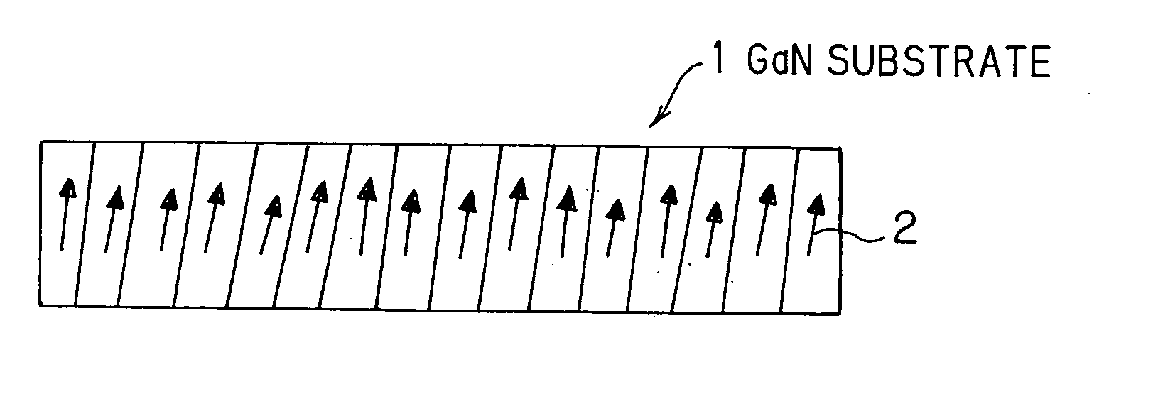
[0070] A plurality of GaN templates are fabricated such that 4 μm Si-doped GaN layer is grown through 20 nm GaN buffer layer on sapphire C-face substrate with a diameter of 2 inches φ by MOVPE. Growth pressure is atmospheric pressure, substrate temperature in buffer layer growth is 600° C., and substrate temperature in epi-layer growth is 1100° C. TMG is used for III group raw material, NH3 for V group raw material, and monosilane for dopant. Carrier gas is mixed gas of hydrogen and nitrogen. Crystal growth rate is 4 μm / h. Carrier concentration of epi-layer is 2×1018 cm−3.

[0071] In all of the GaN templates, the inclination of C-axis in GaN single crystal (aforementioned Si-doped GaN layer) located on the surface of GaN template is measured in plane. The measurement is conducted such that the amount and direction of C-axis inclination is determined based on the positional relationship between shift amount in X-ray diffraction peak position measured while rotating the sample and orie...

example 2

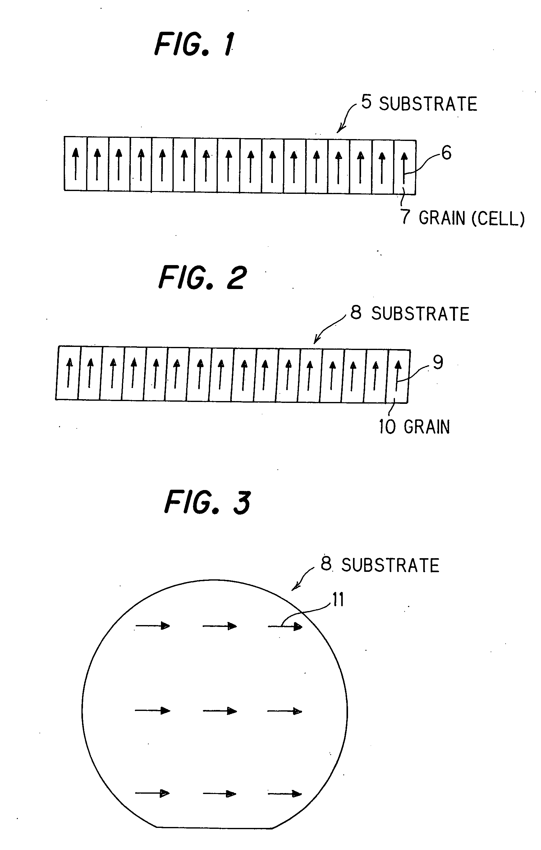
[0076] Ten GaN templates are fabricated such that 1.5 μm Si-doped GaN layer is -grown through 20 nm GaN buffer layer on sapphire C-face substrate with a diameter of 2 inches φ by MOVPE. The sapphire substrate is inclined from C-face by 0.3[deg] in the direction of M-axis. Processing accuracy of “off” is ±0.05 [deg]. Growth pressure is atmospheric pressure, substrate temperature in buffer layer growth is 600° C., and substrate temperature in epi-layer growth is 1100° C. TMG is used for III group raw material, NH3 for V group raw material, and monosilane for dopant. Carrier gas is mixed gas of hydrogen and nitrogen. Crystal growth rate is 4 μm / h. Carrier concentration of epi-layer is 2×1018 cm−3.

[0077] In all of the GaN templates, the inclination of C-axis in GaN single crystal (aforementioned Si-doped GaN layer) located on the surface of GaN template is measured in plane. The measurement is conducted such that the amount and direction of C-axis inclination is determined based on the...

example 3

[0081] 300 μm undoped GaN layer is grown using TMG and NH3 as raw material on commercially available 2-inch diameter single crystal sapphire C-face substrate with “off” of 0.2±0.05 [deg] in the direction of M-axis by MOVPE. 20 nm metal Ti film is deposited on the GaN epi-substrate. Then, it is heat-treated at 1050° C. for 20 min. in H2 flow including 20% NH3 in electric furnace. Thereby, metal Ti film is changed to mesh-like TiN film and a number of voids are formed in the GaN layer. Then, 550 μm GaN is grown thereon in HVPE vessel. In the growth, NH3 and GaCl are used as raw material and N2 is used as carrier gas. The growth conditions are atmospheric pressure and substrate temperature of 1040° C. GaN layer is by itself peeled from the sapphire substrate at the void layer in the cooling process after the growth. Thus, a self-standing GaN substrate is obtained. Using this method, ten self-standing GaN substrates are fabricated under the same conditions.

[0082] All self-standing GaN ...


PUM


Abstract

A III-V group nitride system semiconductor substrate has III-V group nitride system single crystal grown on a hetero-substrate. The III-V group nitride system semiconductor substrate has a flat surface and satisfies the relationship of θ>α, where θ [deg] is given as an average in angles of the substrate surface to low index surfaces closest to the substrate surface measured at a plurality of arbitrary points in plane of the substrate, and a variation range of the measured angles to θ is represented by ±α [deg].

Description

[0001] The present application is based on Japanese patent application No. 2003-368828, the entire contents of which are incorporated herein by reference. BACKGROUND OF THE INVENTION [0002] 1. Field of the Invention [0003] This invention relates to a III-V group nitride system semiconductor substrate. [0004] 2. Description of the Related Art [0005] Nitride system semiconductor materials such as gallium nitride (GaN), indium gallium nitride (InGaN) and gallium aluminum nitride (GaAlN) have a sufficiently wide bandgap and are of direct transition type in inter-band transition. Therefore, they are a great deal researched to be applied to short-wavelength light emitting device. Further, they have a high saturation drift velocity of electron and can use two-dimensional carrier gases in hetero junction. Therefore, they are also expected to be applied to electronic device. [0006] With silicon (Si) or gallium arsenide (GaAs) which is already in popular use, an epitaxial growth layer of sili...

Claims


Application Information

Patent Timeline
IPC IPC(8): C30B23/02C30B25/02C30B29/40H01L21/20C30B29/38H01L29/04H01L29/20H01L29/267
CPCH01L29/2003H01L21/02433H01L21/02576H01L33/16H01L29/267H01L21/0262H01L29/045H01L21/0242H01L21/02458C30B23/02C30B29/40C30B25/02H01L21/0254
Inventor SHIBATA, MASATOMO
Owner SUMITOMO CHEM CO LTD
Why Eureka
Try Eureka