Charge or particle sensing

a particle sensing and charge technology, applied in the field of charge or particle sensing, can solve the problems of limiting the minimum achievable pixel dimension of the type of pixel sensor, limiting the operation and noise performance, and expensive and complex fabrication

Inactive Publication Date: 2005-05-19
EUROPEAN ORGANIZATION FOR NUCLEAR RESEARCH
View PDF11 Cites 34 Cited by
  • Summary
  • Abstract
  • Description
  • Claims
  • Application Information

AI Technical Summary

Benefits of technology

[0011] According to a first aspect of the present invention there is provided a sensing arrangement having a sensor device and amplifier circuitry, the sensor device being constructed and arranged to provide a sensor signal when it receives or one or more charged particles and / or one or more quanta of electromagnetic radiation, the amplifier circuitry having an input node and an output node, the sensor device being connected to said input node for supplying said signal thereto whereby the level at the output node changes, and further having feedback circuitry connecting said input node and said output node for feeding back a portion of the level at the output node for maintaining a first level at the output node in the absence of a said signal from said sensor device, the feedback device being responsive to the change in level of said output node to vary the effect of said feedback circuitry when said level changes to increase the loop gain of said amplifier circuitry.

Problems solved by technology

However, this type of pixel sensor has a limit to the minimum achievable pixel dimensions due to the bump bonding technique.
So far 50 μm×50 μm has been achieved, but it is expensive and complex to fabricate.
Moreover, the hybrid pixel sensor has an input capacitance (100 fF to 200 fF) sufficiently high to limit the operation and noise performance.
This has the disadvantage of generating kTC or reset noise far above the intrinsic electronic noise of the amplifier stage.
Furthermore, the device shown in FIG. 1 is not capable of discriminating between incident quanta (hits) during the integration period.
A major drawback of the conventional bulk silicon sensor is that charge collection is achieved by thermal diffusion of carriers.
This intrinsically limits carrier velocity and thus charge collection is slow> Charge collection is also spread over adjacent pixels and not complete.
This requires a noise floor below 5 e− rms, which cannot be achieved by the conventional APS integrating architectures.
Moreover, the integrating APS architecture of conventional devices cannot measure the timing of particle events, and cannot digitally count each incoming charged particle or X-ray or visible photon.
Conventional circuit architectures for hybrid pixel radiation sensors are generally too large, typically, at best 50 μm×50 μm, and consume too much power, for example 30 to 50 μW, and are consequently not usable for monolithic integration of high density pixel sensors with quantum detection capability.

Method used


Image

  • Charge or particle sensing
  • Charge or particle sensing
  • Charge or particle sensing

Examples


Embodiment Construction

[0085] In the various figures, like reference signs refer to like parts.

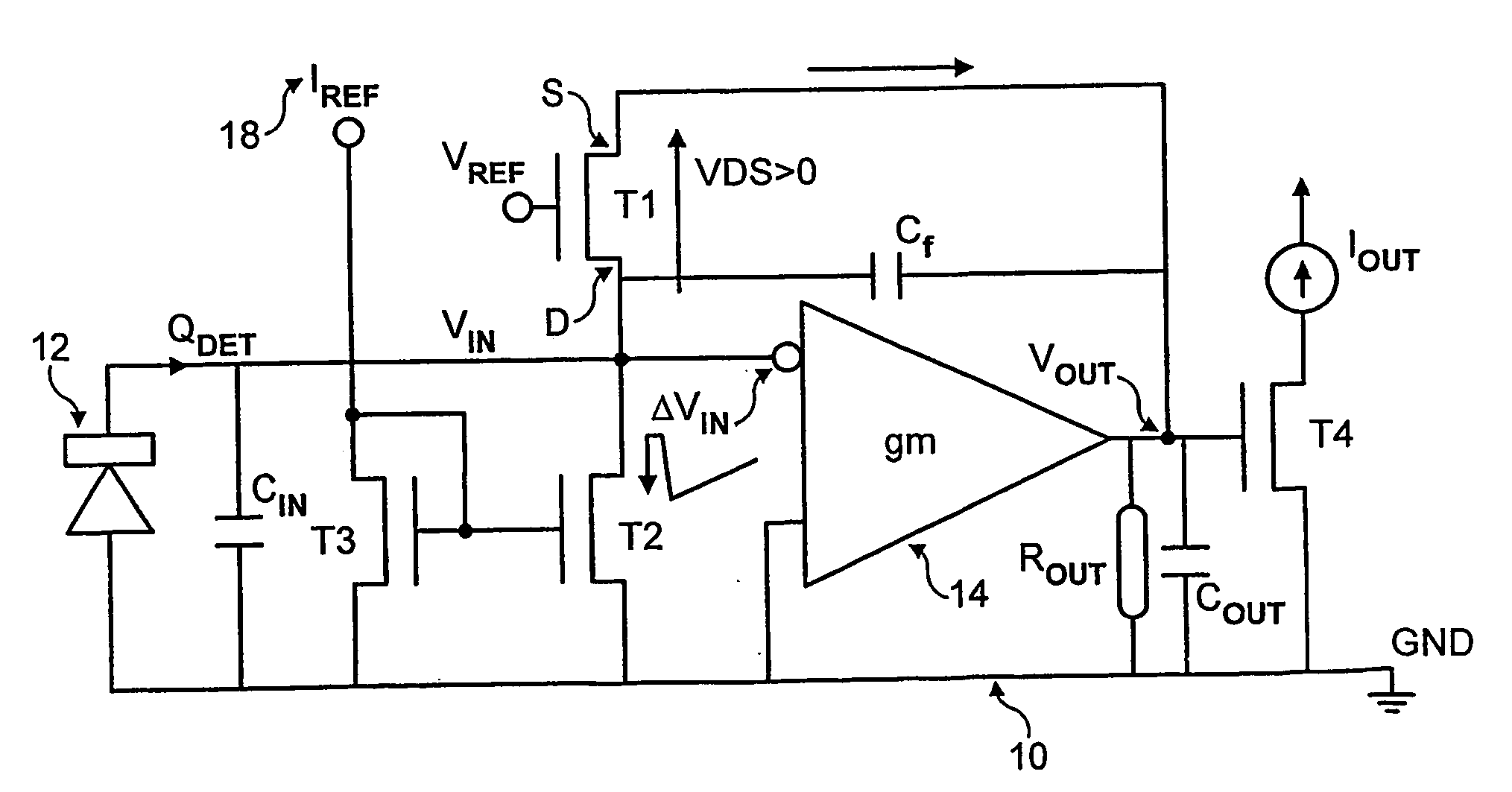
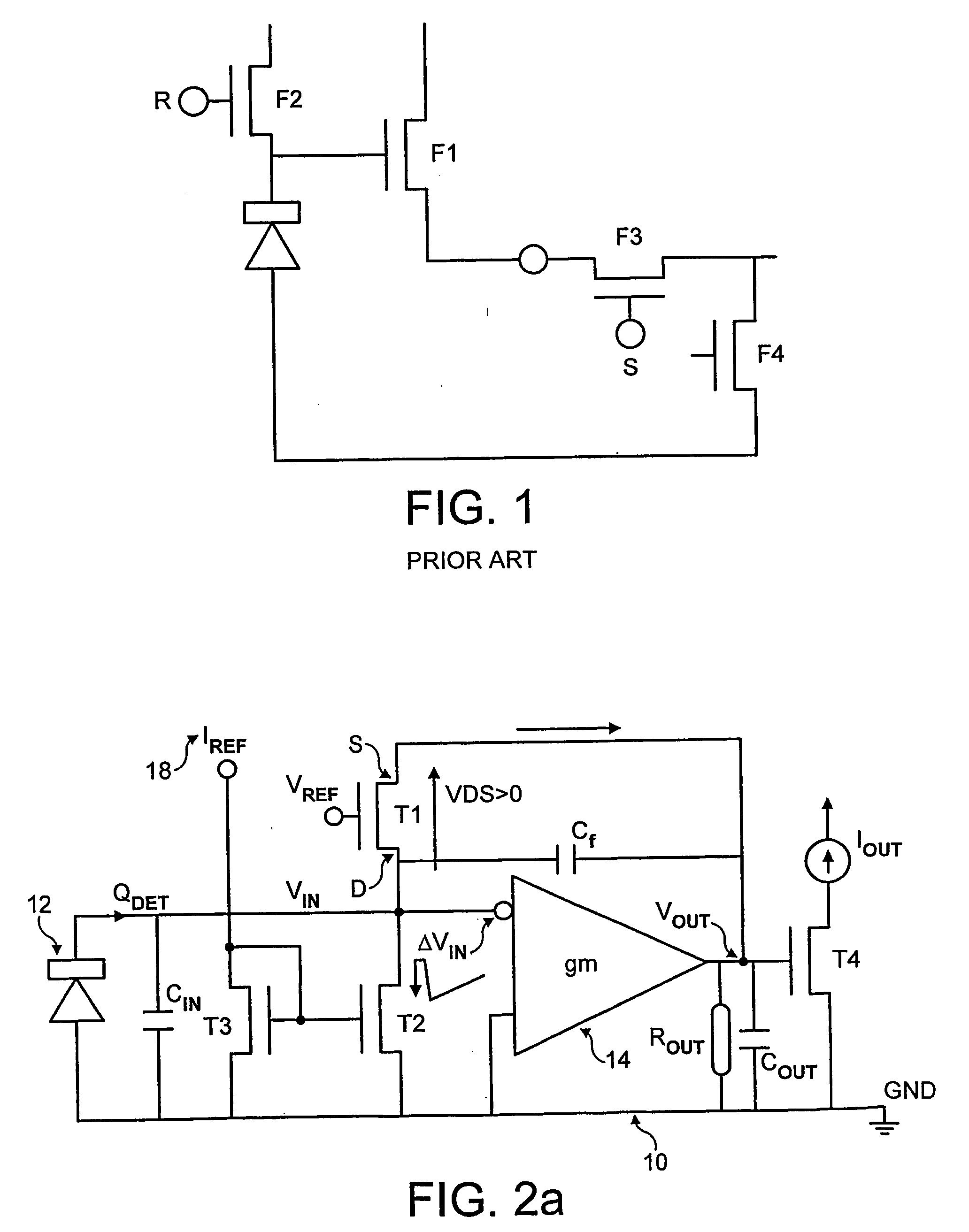
[0086]FIG. 2A shows a simplified schematic block diagram of one sensing device 10, such as a pixel cell, of a Single Particle Detector (SPD) planar array of many such devices, or cells, formed in an integrated circuit. The sensing device 10 has a sensor 12, an inverting transconductance amplifier 14, a current mirror formed from two transistors T2 and T3, a feedback MOSFET transistor T1, and an output MOSFET discriminator transistor T4. The sensor 12 is connected to the input of the amplifier 14. The feedback MOSFET transistor T1 has its main current path connected between the input and the output of the amplifier 14 and the output of the amplifier 14 is fed to the output MOSFET discriminator transistor T4, and is configured to be able to provide negative feedback. The discriminator transistor T4 is driven directly from the output node of the transconductance amplifier 14. The transistor T4 acts as a switch, re...


PUM


Abstract

A sensing arrangement for sensing charged particles and/or quanta of elektromagnetic radiation has a sensor device (12) and amplifier circuitry (14). The sensor device (12) provides a sensor signal to an imput mode (vin) of the amplifier (14) to cause the level at the amplifier output mode (vout) to change. A negative feetback device (T1) responds to the change in level of the output node (Vour) to vary the feedback effect to increase the loop again of said amplifier circuitry (14). A current mirror (T2,T3) resets the input node (vin) to its initil level. Single particle and integrating sensor arrangements are disclosed.

Description

FIELD OF THE INVENTION [0001] The invention relates to a sensing arrangement, a detection system, a macropixel and a method of detecting the arrival of one or more charged particles and / or one or more quanta of electromagnetic radiation. BACKGROUND OF THE INVENTION [0002] Conventional pixel radiation sensors are often based on a hybrid approach in which an electronic circuit is bump bonded to a pixel sensor. [0003] There are a number of types of conventional semiconductor imagers and sensors. One class is based on a hybrid pixel sensor arrangement for two-dimensional single particle detection, or single photon detection. Another class uses monolithic active pixel sensors (APS) that are solid state imagers that provide, for each pixel, radiation-sensing, charge-to-voltage conversion, and a reset function. [0004] The hybrid pixel sensor arrangement is mainly used for IR focal planes, Silicon Pixel arrays for single particle detection, X-ray detection and medical imaging. The hybrid pi...

Claims


Application Information

Patent Timeline
Patent Type & Authority Applications(United States)
IPC IPC(8): G01T1/17G01T1/24H01L27/14H03F3/08H04N3/15H04N5/30
CPCH03F3/087H04N3/155H03F2200/357H03F2200/162H04N25/767H04N25/77H01J37/244H01J37/02
Inventor JARRON, PIERRE
Owner EUROPEAN ORGANIZATION FOR NUCLEAR RESEARCH
Why Eureka
Try Eureka