Semiconductor memory cell and semiconductor memory device

Inactive Publication Date: 2005-06-23
SEMICON ENERGY LAB CO LTD
View PDF15 Cites 4 Cited by
  • Summary
  • Abstract
  • Description
  • Claims
  • Application Information

AI Technical Summary

Benefits of technology

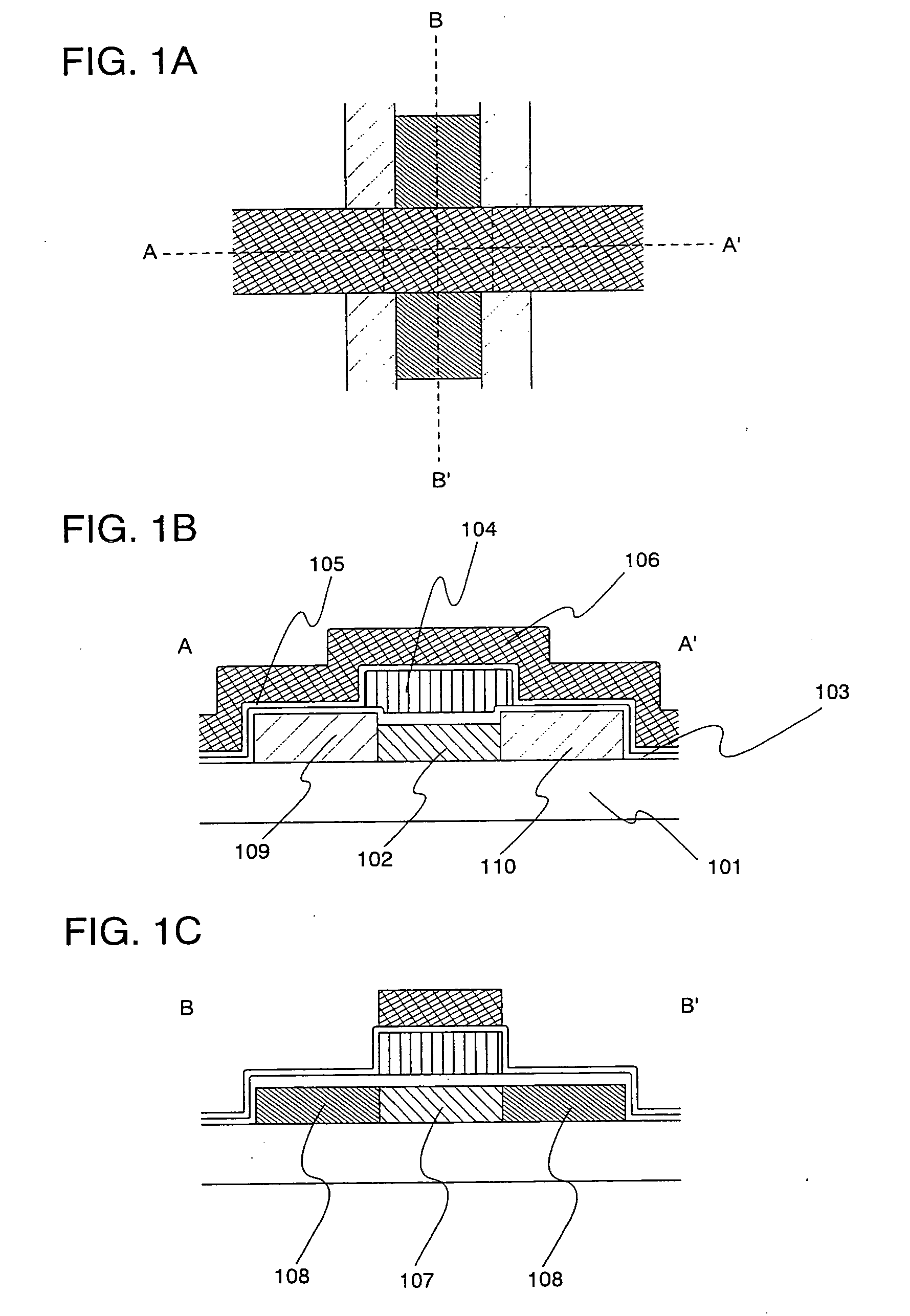
[0041] The present invention described above makes it possible to specify locations of channel formation regions of semiconductor memory cells and TFTs and form crystalline semiconductor films that contain no other grain boundaries than twin crystal in the channel regions. This means that the crystallinity of the channel regions of the TFTs and semiconductor memory cells can be controlled and improv

Problems solved by technology

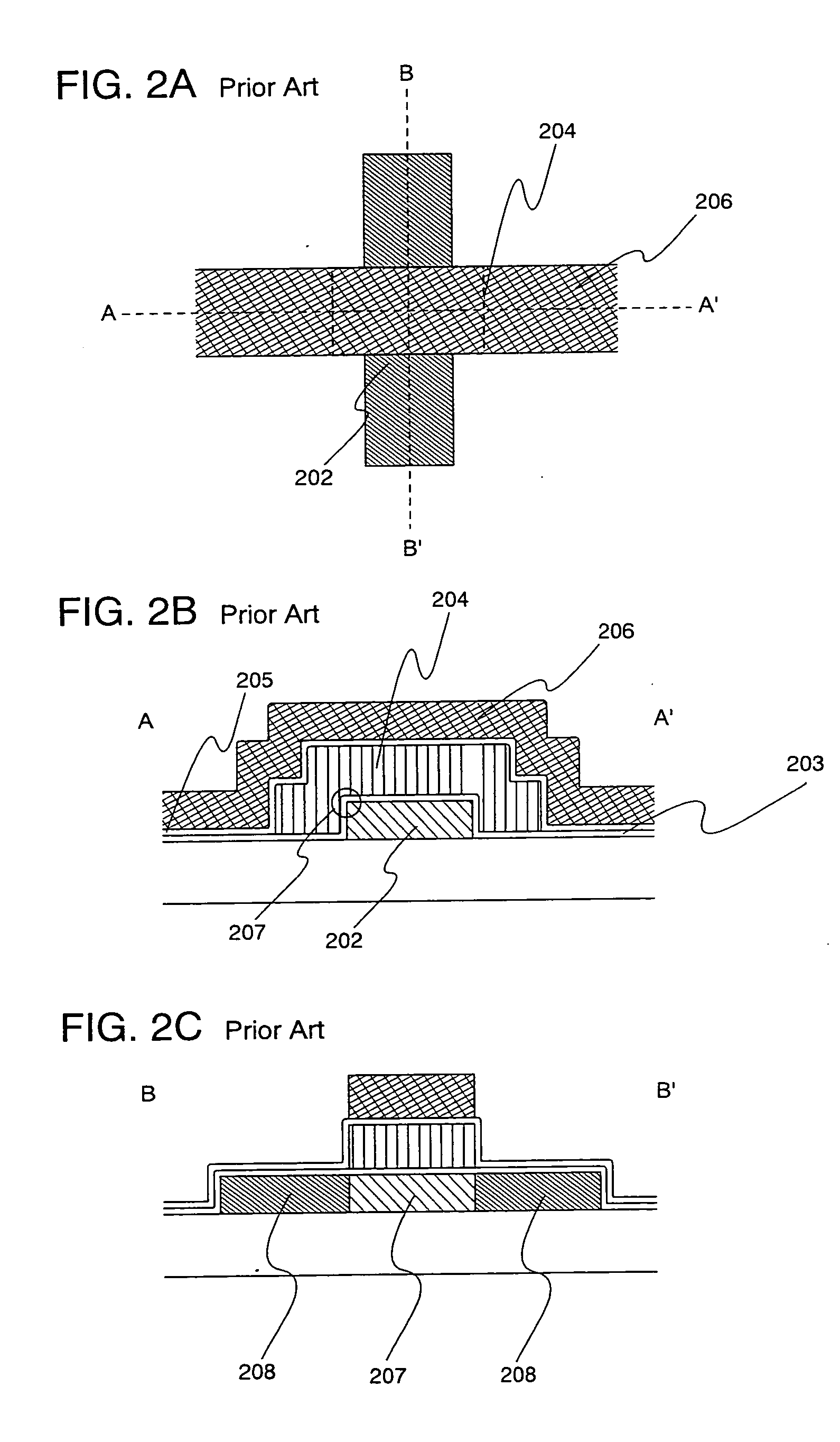
First, regarding the reliability, a semiconductor memory cell has the following structural problem.
In this semiconductor memory cell structure, what causes a problem regarding the reliability is the shape of a semiconductor active layer end 209.
However, when an amorphous semiconductor film formed on a flat surface is crystallized by laser light irradiation, the crystal obtained is polycrystal and it is impossible to control neither positions where grain b

Method used


Image

  • Semiconductor memory cell and semiconductor memory device
  • Semiconductor memory cell and semiconductor memory device
  • Semiconductor memory cell and semiconductor memory device

Examples


embodiment mode 1

[0071] A circuit structure and operation method of a non-volatile memory will be described as an embodiment mode of a semiconductor memory device of the present invention.

[0072] Features of the present invention are in the structure of a semiconductor memory cell and its semiconductor active layer and in the structure and semiconductor active layers of TFTs that constitute peripheral circuits. For the circuit structure and operation method of a memory cell, known techniques are used. This embodiment mode gives a brief description on the circuit structure and operation method of a NOR flash memory as a typical non-volatile memory.

[0073]FIG. 7 is a block circuit diagram of a NOR flash memory having a storage capacity of m×n bits: The NOR flash memory shown in FIG. 7 is composed of a memory cell array 701 and peripheral circuits including an X address decoder 703, a Y address decoder 702, a Y selector 704, and a writing / reading circuit 705. The memory cell array 701 has plural memory...

embodiment mode 2

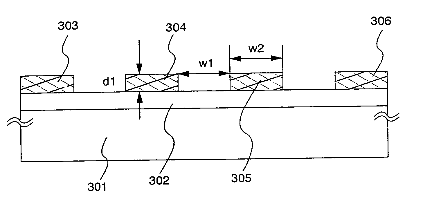
[0082] A method of forming a crystalline semiconductor film in the present invention will be described. The description is given with reference to FIGS. 3A to 6B. In perspective views of FIGS. 3A and 3B, a first insulating film 302 and second insulating films 303 to 306 form stripe pattern concave portions on a substrate 301. Although FIGS. 3A and 3B show three linear concave portions, the number of linear concave portions is not limited thereto.

[0083] The substrate employed is a commercially-available non-alkaline glass substrate, quartz substrate, sapphire substrate, or single crystal or polycrystal semiconductor substrate with its surface covered with an insulating film. Alternatively, a metal substrate with its surface covered with an insulating film may be employed.

[0084] To form the stripe pattern concave portions with a sub-micron level design rule, it is necessary to reduce unevenness on the substrate surface and warpage or contortion of the substrate down to the depth of ...

embodiment mode 3

[0109] Referring to the drawings, a description is given on a mode of manufacturing a semiconductor memory cell and a TFT whose channel formation regions are placed in filling regions of a crystalline silicon film on a base insulating film that has concave portions. The filling regions are portions of the crystalline silicon film that fill the concave portions. In each of the drawings for this embodiment mode, (1) is a top view whereas (2) to (5) are sectional views of several portions in the top view.

[0110] In the mode shown in this embodiment mode, a memory cell array and peripheral circuits are manufactured simultaneously. On the right hand of the drawings is a part of a NOR memory cell array in which semiconductor memory cells are arranged to form a matrix pattern. Shown on the left hand of the drawings as a representative of the peripheral circuits is an inverter composed of an n-channel TFT and a p-channel TFT.

[0111]FIGS. 8A to 8E show a mode in which a first insulating film...


PUM


Abstract

An insulating film with a linear concave portion is formed and a semiconductor film is formed thereon by deposition. The semiconductor film is irradiated with laser light to melt the semiconductor film and the melted semiconductor is poured into the concave portion, where it is crystallized. This makes distortion or stress accompanying crystallization concentrate on other regions than the concave portion. A surface of this crystalline semiconductor film is etched away, thereby forming in the concave portion a crystalline semiconductor film which is covered with side walls of the concave portion from the sides and which has no other grain boundaries than twin crystal. TFTs and memory TFTs having this crystalline semiconductor film as their channel regions are highly reliable, have high field effect mobility, and are less fluctuated in characteristic. Accordingly, a highly reliable semiconductor memory device which can operate at high speed is obtained.

Description

BACKGROUND OF THE INVENTION [0001] 1. Field of the Invention [0002] The present invention relates to a semiconductor memory cell, specifically, a thin film transistor having an electric charge accumulating layer. The present invention also relates to a semiconductor memory device in which a thin film transistor having an electric charge accumulating layer and a thin film transistor are formed on a substrate having an insulating surface. [0003] 2. Description of the Related Art [0004] EEPROM (Electrically Erasable and Programmable Read Only Memory) and flash memory are known as representatives of semiconductor non-volatile memories. Unlike major semiconductor memories such as DRAM (Dynamic Random Access Memory) and SRAM (static RAM), EEPROM and flash memory do not lose data when power is turned off since they are non-volatile. They are also superior to magnetic disc, which is another representative non-volatile memory, in such characteristics as high integration degree, withstandingn...

Claims


Application Information

Patent Timeline
IPC IPC(8): H01L21/28H01L21/336H01L21/77H01L21/8247H01L21/84H01L27/105H01L27/115H01L27/12H01L29/04H01L29/786H01L29/788
CPCH01L21/28273H01L27/1281H01L27/115H01L27/11521H01L27/11526H01L27/11546H01L27/11568H01L27/12H01L29/04H01L29/42332H01L29/66757H01L29/78603H01L29/78675H01L29/78696H01L29/7881H01L29/792H01L27/105H01L29/40114H10B41/40H10B41/49H10B43/30H10B69/00H10B41/30
Inventor KATO, KIYOSHIISOBE, ATSUOMIYAIRI, HIDEKAZUYAMAZAKI, SHUNPEI
Owner SEMICON ENERGY LAB CO LTD
Why Eureka
Try Eureka