Structure of imprint mold and method for fabricating the same

a technology of imprint mold and structure, which is applied in the direction of photomechanical treatment originals, instruments, photomechanical equipment, etc., can solve the problems of nano-imprint lithography application, application of nano-imprint lithography, and high process time and production costs, and achieves easy removal of imprinted materials, better anti-friction

a technology of imprint mold and structure, which is applied in the direction of photomechanical treatment originals, instruments, photomechanical equipment, etc., can solve the problems of nano-imprint lithography application, application of nano-imprint lithography, and high process time and production costs, and achieves easy removal of imprinted materials, better anti-friction

US20050170292A1Inactive Publication Date: 2005-08-04IND TECH RES INST

Image

  • Structure of imprint mold and method for fabricating the same
  • Structure of imprint mold and method for fabricating the same
  • Structure of imprint mold and method for fabricating the same

Examples


Embodiment Construction

[0020] Matched with corresponding drawings, the preferable embodiments of the invention are presented as following and hope they will benefit your esteemed reviewing committee members in reviewing this patent application favorably.

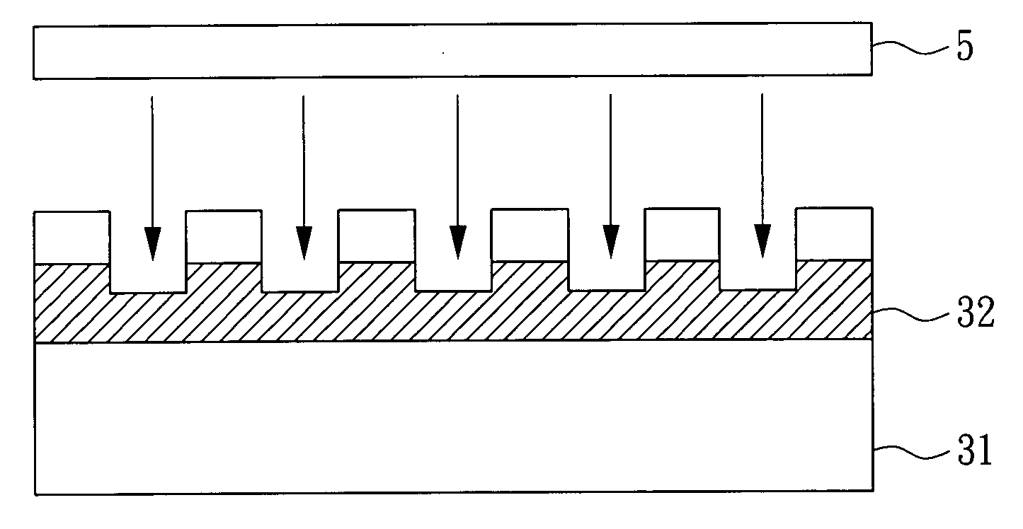
[0021] Please refer to FIG. 3A to FIG. 3D, which are the schematic views showing the best embodiment of the method for fabricating the imprint mold of the present invention. Firstly, a substrate 31 is provided; wherein, the material of the substrate 31 can be various, such as silicon wafer, quartz, sapphire, tungsten, molybdenum, titanium, iridium, magnesia and so on according to the different applications of the nano-imprint process. Then a diamond film 32 is formed on the substrate 31; wherein the material of the diamond film 32 can be diamond or diamond like carbon (DLC), and the forming method thereof can be the chemical vapor deposition (CVD). The thickness of the diamond film 32 needs not be too thick, just only thicker than what the imprint process...


PUM

PropertyMeasurementUnit
structureaaaaaaaaaa
optical wavelengthaaaaaaaaaa
temperatureaaaaaaaaaa

Abstract

The present invention is related to a structure of an imprint mold and a method for fabricating the same, which can be used in the field of nano-imprint lithography. Firstly, a diamond film and a photoresist film are successively formed onto a substrate; wherein the photoresist film is more capable of anticorrosion than the diamond film. Then an energy beam lithography system is provided to make the photoresist film form a photoresist mask with particularly arranged patterns. Because of the etching selectivity between the diamond film and the photoresist film, on the surface of the diamond film can be easily formed a pattern with recessions and protrusions according to the photoresist mask by dry etching method. Thus an imprint mold characterized as better antifriction and easily taking off from imprinted materials is completed.

Description

1. FIELD OF THE INVENTION [0001] The present invention relates to a structure of imprint mold and the method for fabricating the same, in particular to a nano-imprint mold made of diamond material and the fabricating method thereof in order to extend the mold lifetime and reduce the manufacture cost when applying the nano-imprint process technology. 2. BACKGROUND OF THE INVENTION [0002] Along with the semiconductor manufacturing process entering the era of nanotechnology, the traditional photolithography is confronted with the predicament, the physical extremity of the optical wavelength. Therefore, finding a substitution technology with low cost and high production thus becomes the key point in the next generation researches. Wherein, the nano-imprint lithography possessing the characters of thin line width, low cost, and high production is considered as the main stream of the next generation lithography technology. Meanwhile, the related patents are quickly accumulated. [0003] The...

Claims


Application Information

Patent Timeline
04 Aug 2005
Publication
US20050170292A1
IPC
B32B9/00; G03F7/00
CPC
B82Y10/00; Y10T428/30; G03F7/0002; B82Y40/00
Inventors
TSAI, HUNG-YIN; WU, CHIH-HUNG