Polymer, resist composition and patterning process

a technology of resist material and composition, applied in the field of polymer, resist composition and patterning process, can solve the problems of resist material having substantial line density dependency, inability to use resist material in an industrially acceptable manner, and inability to produce desired patterns in both dense and sparse regions at the same exposure, so as to improve resolution and proximity bias, the effect of minimizing absorption

Inactive Publication Date: 2005-09-22
SHIN ETSU CHEM IND CO LTD
View PDF14 Cites 16 Cited by
  • Summary
  • Abstract
  • Description
  • Claims
  • Application Information

AI Technical Summary

Benefits of technology

[0014] The inventive resist composition prepared using the inventive polymer lends itself to micropatterning with electron beams or deep UV since it is sensitive to high-energy radiation and is improved in resolution and proximity bias. Especially because of the minimized absorption at the exposure wavelength of an ArF or KrF excimer laser, the composition can be processed by photolithography using such a laser, to form a finely defined complex pattern. The polymer is thus best suited as the base resin in resist compositions for VLSI fabrication.

Problems solved by technology

For the above-described resist compositions, however, there is a common problem of line density dependency that when a pattern to be transferred includes dense and sparse regions, it is impossible to produce the desired pattern in both the dense and sparse regions at the same exposure.
Then at the very fine pattern size for which an ArF excimer laser is actually used, a resist material having substantial line density dependency cannot be used in an industrially acceptable manner because isolated lines can disappear.

Method used


Image

  • Polymer, resist composition and patterning process
  • Polymer, resist composition and patterning process
  • Polymer, resist composition and patterning process

Examples


synthesis example 1

[0398] Synthesis of Polymer 1

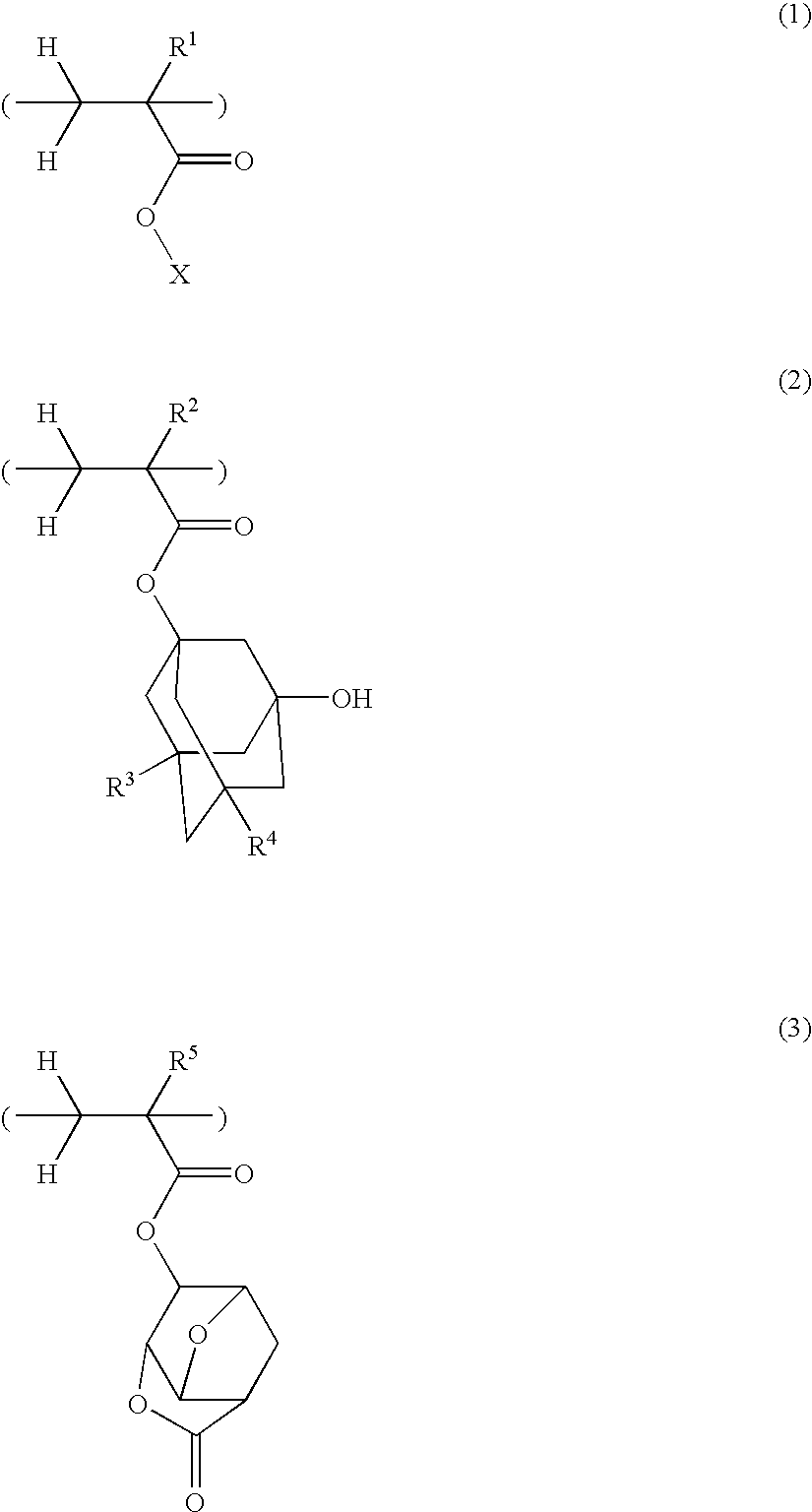
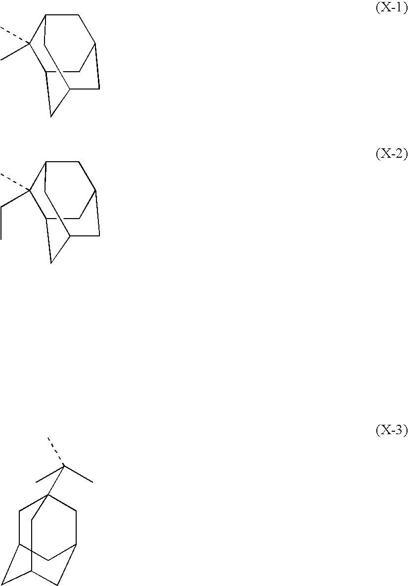
[0399] There were combined 14.8 g of 2-ethyl-2-adamantyl methacrylate, 10.0 g of hydroxyadamantyl methacrylate, 15.2 g of 4,8-dioxatricyclo[4.2.1.03,7]nonan-5-on-2-yl methacrylate, and 120 g of 2-butanone. The mixture was heated at 80° C., after which 1.2 g of dimethyl 2,2′-azobisisobutyrate was added. The mixture was stirred for 10 hours while keeping at 80° C. The reaction mixture was cooled to room temperature and thereafter, added dropwise to 600 g of n-hexane, with vigorous stirring. Solids settled out and were separated by filtration and dried at 40° C. in vacuum for 15 hours. There was obtained a polymer in while powder solid form, designated Polymer 1. The amount was 32.4 g and the yield was 81%. The polymer had a weight average molecular weight (Mw) of 6,800 as measured by gel permeation chromatography (GPC) using polystyrene standards.

example 1

[0419] Using Polymer 1 obtained in Synthesis Example 1, a resist material was prepared according to the composition: [0420] (A) 80 parts by weight of Polymer 1 as the base resin, [0421] (B) 2.0 parts by weight of triphenylsulfonium nonafluorobutanesulfonate as the acid generator, [0422] (C) 640 parts by weight of propylene glycol monomethyl ether acetate as the solvent, and [0423] (D) 0.25 part by weight of triethanolamine as the organic nitrogen-containing compound.

This was passed through a Teflon® filter having a pore diameter of 0.2 μm.

[0424] The resist material was spin coated on a silicon wafer having an antireflection film (ARC29A by Nissan Chemical Co., Ltd., 78 nm) coated thereon and heat treated at 130° C. for 60 seconds, forming a resist film of 300 nm thick. The resist film was exposed to light in an ArF excimer laser stepper (Nikon Corp., NA=0.68), heat treated (PEB) at 120-130° C. for 60 seconds, cooled down to 23° C., and puddle developed in a 2.38% aqueous solution...

example 9

[0427] Using Polymer 9 obtained in Synthesis Example 9, a resist material was prepared according to the composition: [0428] (A) 80 parts by weight of Polymer 9 as the base resin, [0429] (B) 2.0 parts by weight of triphenylsulfonium nonafluorobutanesulfonate as the acid generator, [0430] (C) 640 parts by weight of propylene glycol monomethyl ether acetate as the solvent, and [0431] (D) 0.12 part by weight of triethanolamine as the organic nitrogen-containing compound.

This was passed through a Teflon® filter having a pore diameter of 0.2 μm.

[0432] The resist material was spin coated on a silicon wafer having an antireflection film (ARC29A by Nissan Chemical Co., Ltd., 78 nm) coated thereon and heat treated at 105° C. for 60 seconds, forming a resist film of 295 nm thick. The resist film was exposed to light in an ArF excimer laser stepper (Nikon Corp., NA=0.68), heat treated (PEB) at 120-130° C. for 60 seconds, cooled down to 23° C., and puddle developed in a 2.38% aqueous solution...


PUM

PropertyMeasurementUnit
sizeaaaaaaaaaa
thicknessaaaaaaaaaa
wavelengthaaaaaaaaaa

Abstract

A polymer comprising repeat units of formulae (1) to (3) increases a dissolution rate in an alkali developer under the action of an acid.
R1, R2 and R5 are H or CH3, R3 and R4 are H or OH, and X is a tertiary alkyl group having an adamantane structure. A resist composition comprising the inventive polymer has a sensitivity to high-energy radiation, improved resolution and minimized proximity bias and lends itself to micropatterning with electron beams or deep UV for VLSI fabrication.

Description

CROSS-REFERENCE TO RELATED APPLICATION [0001] This non-provisional application claims priority under 35 U.S.C. §119(a) on Patent Application No. 2004-082327 filed in Japan on Mar. 22, 2004, the entire contents of which are hereby incorporated by reference. TECHNICAL FIELD [0002] This invention relates to (i) a novel polymer for resist use, (ii) a resist composition comprising the polymer as a base resin for use in the micropatterning technology, and (iii) a patterning process using the resist composition. BACKGROUND OF THE INVENTION [0003] While a number of recent efforts are being made to achieve a finer pattern rule in the drive for higher integration and operating speeds in LSI devices, deep-ultraviolet lithography is thought to hold particular promise as the next generation in microfabrication technology. In particular, photolithography using a KrF or ArF excimer laser as the light source is strongly desired to reach the practical level as the micropatterning technique capable o...

Claims


Application Information

Patent Timeline
Patent Type & Authority Applications(United States)
IPC IPC(8): C08F220/26G03F7/033C08F220/28G03C1/492G03F7/039H01L21/027
CPCG03F7/0397C08F220/26C02F1/442C02F1/441A23L2/38A23L33/00A23V2002/00A23V2300/34A23V2300/50A23V2250/1638
Inventor HASEGAWA, KOJINISHI, TSUNEHIROTACHIBANA, SEIICHIRO
Owner SHIN ETSU CHEM IND CO LTD
Why Eureka
Try Eureka