Siloxane epoxy polymers for low-k dielectric applications
a technology of epoxy polymers and dielectrics, applied in the field of dielectric materials, can solve the problems of limiting circuit speed, unable to meet the needs of the semiconductor industry, and reducing the ic frequency, so as to achieve better performan
- Summary
- Abstract
- Description
- Claims
- Application Information
AI Technical Summary
Benefits of technology
Problems solved by technology
Method used
Image
Examples
example 1
[0039] N-type, 4-inch silicon wafers having a resistivity of 0-0.02 ohm-cm for MIM (Metal-Insulator-Metal) structures were used as the semiconductor substrates. After standard RCA cleaning an adhesion promoter (HMDS) was spin-coated onto each wafer at 3000 rpm for 40 sec. The wafers were then annealed in air at 100° C. for 10 min. A siloxane epoxy polymer solution containing formula (IIB), wherein the ratio of p to q was about 2:1, was spin-coated onto each wafer at 3000 rpm for 100 sec to a thickness of 0.5 μm. The polymeric film / wafers were dried under vacuum of 10−3 torr for 1 hour at 100° C. The polymer films were then cured at 165° C. under nitrogen gas flow for 2 hours to cross-link the polymer.
example 2
[0040] The procedure of Example 1 was followed. After curing, the polymer films were subjected to a thermal anneal at 250° C. under nitrogen gas flow for 2 hours.
[0041] The dielectric constants of the polymer films from Examples 1 and 2 were determined by measuring the capacitance of the polymer films (i.e., Metal-Insulator-Semiconductor (MIS) capacitor devices, Metal-Insulator-Metal (MIM) capacitor devices, and C-V techniques). The polymer was regularly shown to have a dielectric constant below 2.65. However, a dielectric constant as low as 2.2 has been measured for thinner films ranging from about 0.02 μm to about 0.09 μm.
example 3
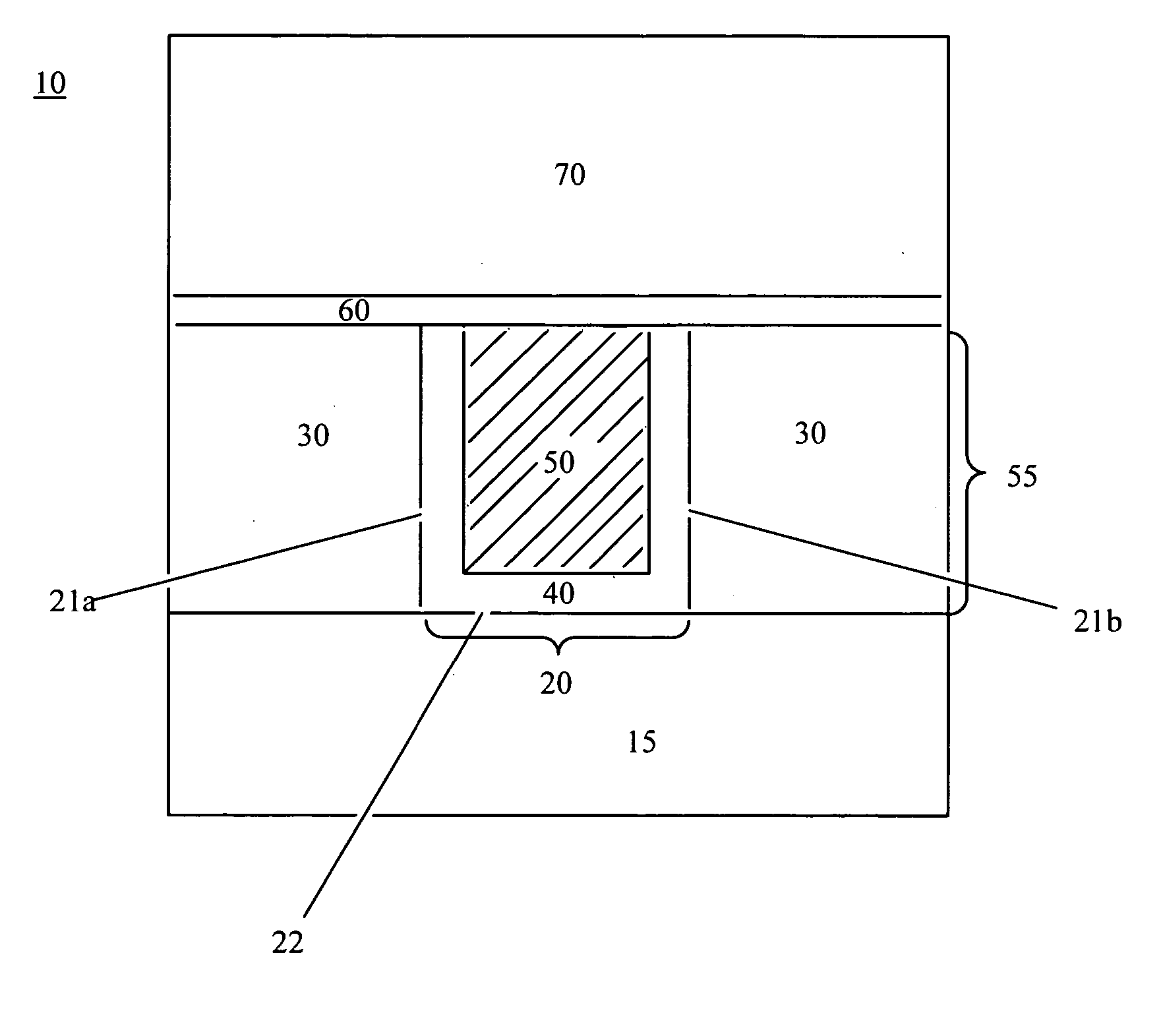
[0042] Metal-Insulator-Semiconductor (MIS) capacitor structures were prepared from the samples of Example 1 by depositing a copper metal film directly onto the polymer layer of each sample prior to drying and curing. Copper served as an electrode in the structures. The copper metal thin films were deposited to a thickness of 0.3 μm using sputtering or e-beam evaporation. After drying and curing, as described in Example 1, the samples were then annealed at 250° C. under nitrogen gas for 1 hr.
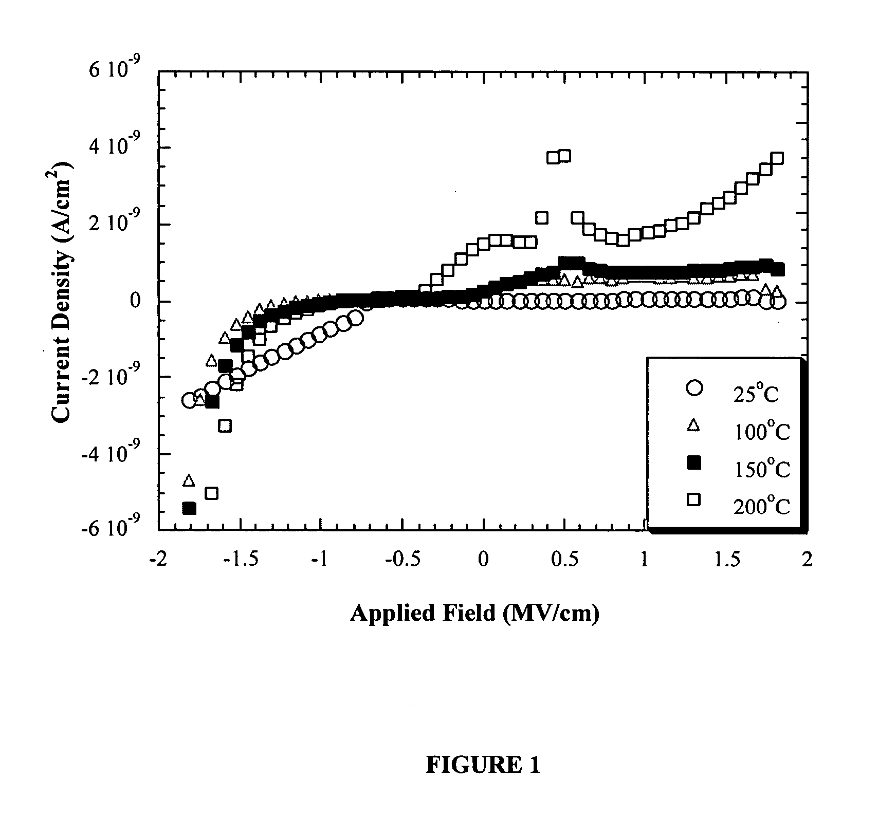
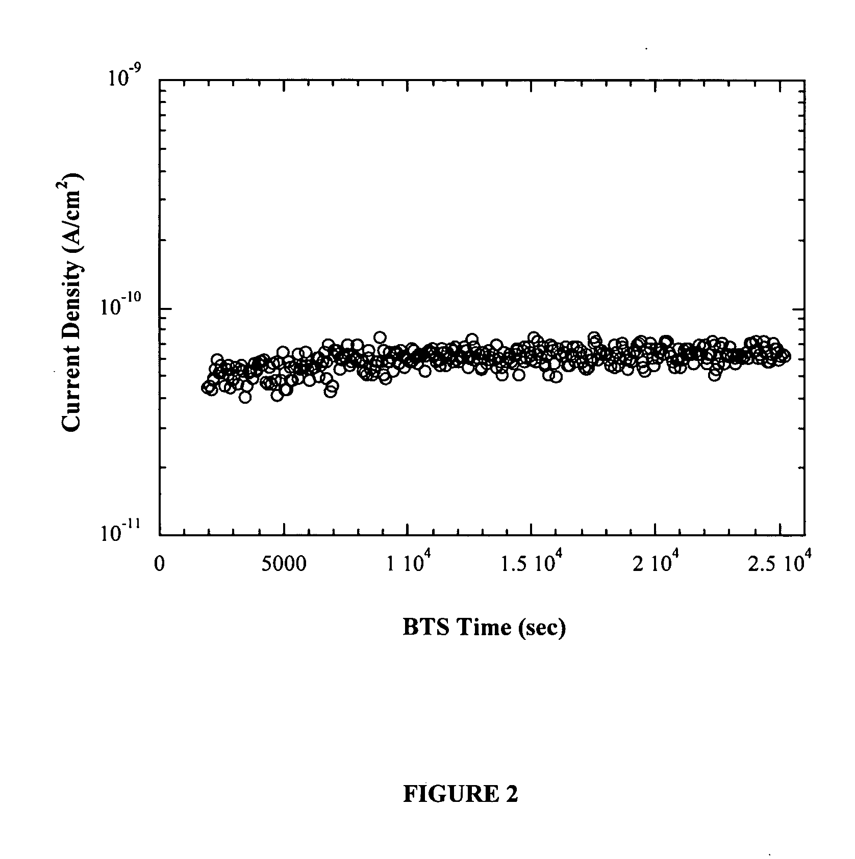
[0043] The electrical stability of the siloxane epoxy polymer (IIB) used in the capacitors of Example 3 was examined by doing I-V measurements on the films at 25° C. and higher temperatures. The measured current (I) was divided by the electrode area to get current density (J), and the voltage (V) was divided by the film thickness (0.5 μm) to get applied electrical field (E). The J (A / cm2) vs. E (MV / cm) plot for the polymer is shown in FIG. 1 and indicates that the leakage current density through...
PUM
| Property | Measurement | Unit |
|---|---|---|
| Temperature | aaaaa | aaaaa |
| Thickness | aaaaa | aaaaa |
| Thickness | aaaaa | aaaaa |
Abstract
Description
Claims
Application Information


