Conductive ink composition, reflective member, circuit substrate, and electronic apparatus

a technology of reflective members and inks, applied in the direction of inks, natural mineral layered products, synthetic resin layered products, etc., can solve the problems of poor material efficiency, long manufacturing time, and high disposal costs, and achieve excellent surface smoothness, excellent surface smoothness, and improved adhesiveness to an application target

Inactive Publication Date: 2005-12-29
SHARP KK +1
View PDF10 Cites 26 Cited by
  • Summary
  • Abstract
  • Description
  • Claims
  • Application Information

AI Technical Summary

Benefits of technology

[0014] The present invention is made in light of the conventional problems, and its object is to provide (i) a conductive ink composition, which allows restraint of the metal grain growth as compared with the conventional conductive ink, such as the silver ink, using metal fine particles each made of silver; (ii) a reflective member using the conductive ink composition; and (iii) a circuit substrate using the conductive ink composition, and (iv) an electronic apparatus using the conductive ink composition. Additional object of the present invention is to provide (i) a conductive ink composition, which is improved in terms of adhesiveness to an application target as compared with a conventional conductive ink, such as the silver ink, using metal fine particles consisting of only a noble metal; (ii) a reflective member using the conductive ink composition; and (iii) a circuit substrate using the conductive ink composition; and (iv) an electronic apparatus using the conductive ink composition. Another additional object of the present invention is to provide (i) a conductive ink composition allowing restraint of the metal grain growth, and accordingly allowing formation of a film having excellent surface smoothness; (ii) a circuit substrate having a metal layer having excellent surface smoothness rendered by restraining the metal grain growth; (iii) an electronic apparatus having such a metal layer; and (iv) a reflective member having such a metal layer. Still another additional object of the present invention is to provide (i) a conductive ink composition allowing restraint of the metal grain growth, and accordingly allowing formation of a film having excellent reflective efficiency; (ii) a circuit substrate having a metal layer having excellent reflective efficiency rendered by restraining the metal grain growth; (iii) an electronic apparatus having such a metal layer; and (iv) a reflective member having such a metal layer.
[0015] The present inventors diligently studied in order to solve the conventional problems, and found that: alloying of a noble metal and an additional metal other than a noble metal allows restraint of the property of the noble metal, and use of protective colloids allows restraint of the metal grain growth occurring in portions containing a larger amount of the noble metal as compared with surroundings. Further, the present inventors found that use of protective colloids made of at least two organic compounds allows effective restraint of the metal grain growth, and accordingly allows improvement of the adhesiveness to the application target, of the film surface smoothness, and of the reflective efficiency as compared with the conventional technique does. The present inventors further studied and found that further devising of the protective colloids in the conductive ink composition allows restraint of the metal grain growth as compared with the conventional technique, (i) even in regions containing a small amount of the additional metal, and (ii) even in cases where the metal fine particles are made of only one noble metal. With this, the adhesiveness, the film surface smoothness, and the reflective efficiency are improved.
[0019] With the arrangements, the conductive ink composition includes the solid material including the metal fine particles coated with the protective colloids each made of at least two organic compounds, the metal fine particles consisting of a plurality of metals, at least one of which is a noble metal. A specific example of such metal fine particles is metal fine particles consisting of an alloy containing at least a noble metal. The use of such a conductive ink composition allows restraint of the metal fine grain growth as compared with the use of the conventional silver conductive ink using the metal fine particles consisting of only silver; and accordingly allows formation of a metal layer (metal film) having excellent surface smoothness, better adhesiveness to the application target, and better reflective efficiency as compared with the conventional silver conductive ink does.
[0025] The protective colloids allow very effective restraint of the grain growth. Therefore, even when the conductive ink composition according to the present invention uses the metal fine particles consisting of only the noble metal, the metal grain growth is restrained as compared with the conventional conductive ink, such as the silver ink, obtained by dispersing, in the organic solvent, the metal fine particles consisting of the noble metal. This allows formation of a metal layer (metal film) having excellent surface smoothness, better adhesiveness to the application target as compared with the conventional metal layer. Therefore, the arrangements above make it possible to provide a conductive ink composition allowing formation of a metal layer having low electric resistance, particularly, formation of a wire having low electric resistance and / or an electrode having low electric resistance. Further, the metal grain growth restraint by the conductive ink composition allows formation of a metal layer having excellent reflective efficiency. Therefore, the arrangements make it possible to provide the conductive ink composition allowing formation of a reflective member which is excellent in terms of surface smoothness, adhesiveness to the application target, and reflective efficiency. The metal layer is especially suitably used for a reflective electrode or the like.
[0029] Each metal layer such as the wire, the electrode, the reflective member, and the like is obtained by drying or heating (e.g., baking) the conductive ink composition according to the present invention. Therefore, the metal grain growth is restrained in the metal layer as compared with that in the metal layer made from the conventional ink such as silver ink, and the metal layer accordingly has excellent surface smoothness, and excellent adhesiveness to the application target. Therefore, the metal layer has lower resistance than the metal layer made from the conventional conductive ink, and has excellent reflective efficiency. So, the arrangements make it possible to provide highly reliable reflective member, circuit substrate, and electronic apparatus, each of which has the metal layer whose surface smoothness is excellent and whose adhesiveness is improved by the restraint of metal grain growth as compared with the metal layer made from the conventional conductive ink.

Problems solved by technology

However, such a conventional manufacturing method suffers from the following problems (1) and (2): (1) the repeated film forming and the repeated etching cause efficiency in use of materials to be bad, and require an expensive disposal cost of many generated waste products such as an etching solution, and require long manufacturing time; and (2) immeasurable equipment cost is required for manufacture of a circuit substrate that has been demanded to be bigger in recent years.
Such immeasurable equipment cost is required because the manufacture of the circuit substrate requires many vacuum apparatuses such as (i) a film forming apparatus used in each film forming step, and (ii) a processing apparatus such as an etching apparatus.
In other words, the noble metal has poor adhesiveness to the substrate.
However, in cases where the paste using the aforementioned silver particles is printed in accordance with the inkjet method or where the paste is applied, such a striking effect cannot be expected during the film forming process.
This reduces the adhesiveness to the priming material such as the glass substrate.
Moreover, in cases where a silver film is formed on a glass substrate, grain growth is noticeable at a baking temperature of approximately 250° C. This causes a smooth surface to be rough, with the result that the surface becomes whitish.
That is, such high temperature baking causes deterioration in the surface smoothness of the formed silver film, and makes it difficult for the formed silver film to be used as a wire just the way as the silver film is.
However, as is the case with the aforementioned case using the silver particles, the grain growth property of the noble metal also causes the surface of the film to be rough, with the result that the surface smoothness is deteriorated.
As such, the grain growth of the noble metal causes deterioration of the surface smoothness, and the deterioration causes various problems.
Further, the film discontinuity caused by the surface deterioration gives rise to the aforementioned top-bottom leakage with a storage capacitor electrode.
With this, the storage capacitor does not possibly work as a capacitor.

Method used


Image

  • Conductive ink composition, reflective member, circuit substrate, and electronic apparatus
  • Conductive ink composition, reflective member, circuit substrate, and electronic apparatus
  • Conductive ink composition, reflective member, circuit substrate, and electronic apparatus

Examples


example 1

[0338] (Hexanoic Acid+Docosanoic Acid+Octylamine)

[0339] A sodium borohydride-2-propanol solution was prepared by adding 15 mmol of sodium borohydride to 2-propanol; (550ml) and stirring the mixture for 3 hours at 80° C.

[0340] Meanwhile, a metallic salt solution was prepared by adding and dissolving, to 2,2,4-trimethylpentane (1.05L), (A) octylamine (150 mmol) as the amine, (B) hexanoic acid (68 mmol) and docosanoic acid (8 mmol) as carboxylic acids, and indium acetate (0.3 mmol) and silver acetate (15 mmol) which are metal compounds.

[0341] Thereafter, to the metallic salt solution, the sodium borchydride-2-propanol solution was dropped at a rate of 10 ml / min. After the dropping, the mixture was stirred for 60 minutes and then concentrated by an evaporator. As a result of this, a brown solution was obtained. Then methanol (1 L) was added to the brown solution, so that a conductive ink composition was generated as a brown precipitation. This precipitation was collected by suction f...

example 2

[0343] (Hexanoic Acid+Naphthenic Acid+Octylamine)

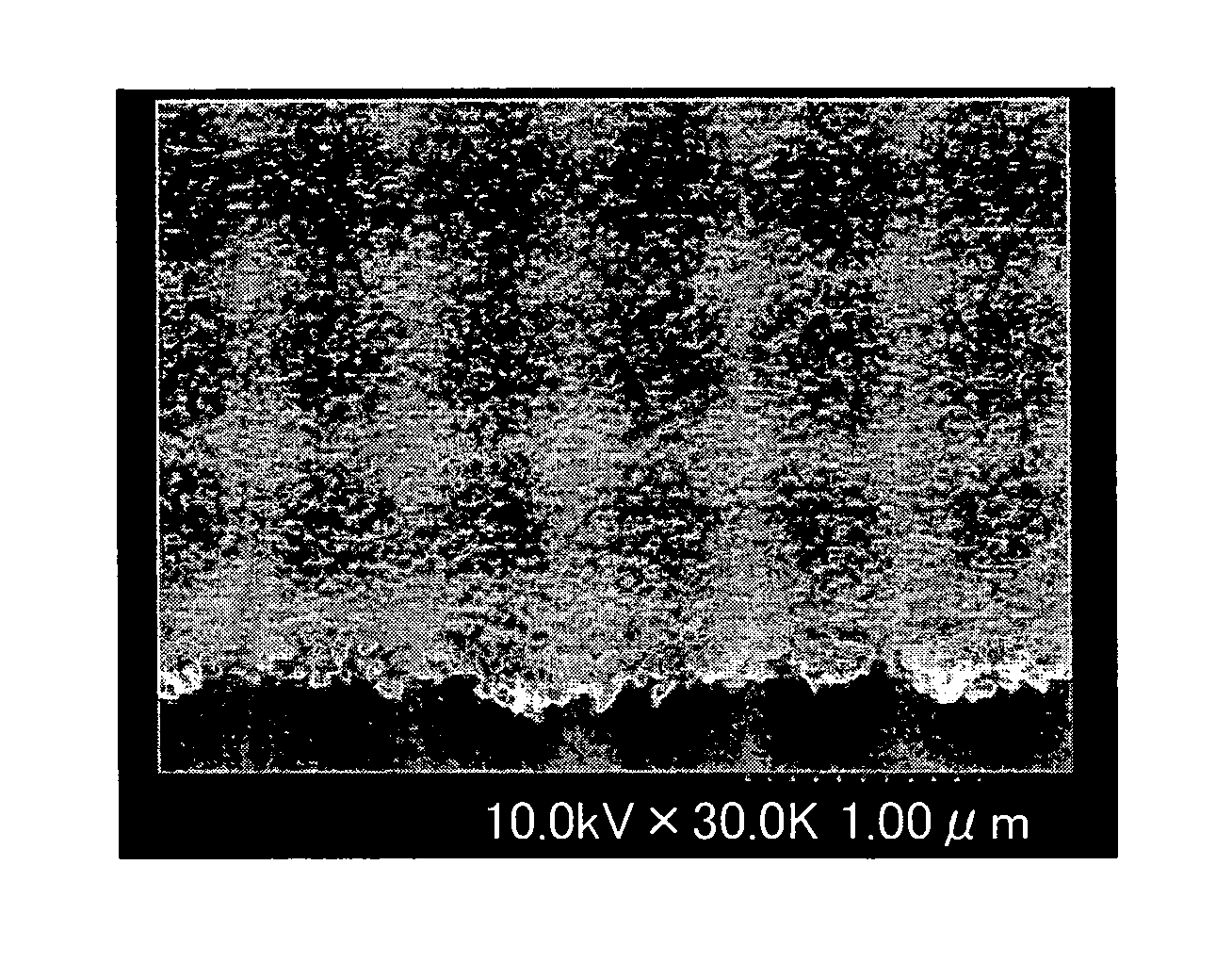
[0344] A silver-indium conductive ink was manufactured in the same conditions as in Example 1, except that docosanoic acid (8 mmol) as the carboxylic acids in (B) was replaced with naphthenic acid (2.025 g roughly equivalent to 8 mmol) whose average molecular mass was about 270, so that a film was formed on a non-alkali glass substrate. The film obtained as a result of the baking was 355 nm thick, and its volume resistivity was 9.8 μΩ·cm. The adhesiveness between the film and the substrate was good, i.e. passed the tape peel test. The rate of indium in the film was 1.0 atomic %. The center line average roughness Ra was 3.2 nm, indicating that the film was flat and smooth. Also, the shape of the film surface did not change after being exposed to an N2 gas atmosphere for 60 minutes at 300° C., i.e. the film exhibited excellent heat resistance. According to the measurement of the naphthenic acid by a GC (gas chromatography) / MS(mass spec...

example 3

[0345] (Hexanoic Acid+Octylamine)

[0346] A silver-indium conductive ink was manufactured in the same conditions as in Example 1, except that docosanoic acid was not added and an amount of the hexanoic acid was increased to 76 mmol (i.e. only the hexanoic acid was adopted as the carboxylic acids in (B)), so that a film was formed on a non-alkali glass substrate. The film obtained as a result of the baking was 508.1 nm thick, and its volume resistivity was 12.5 μΩ·cm. The rate of indium in the film was 0.1 atomic %, and the center line average roughness Ra was 38.2 nm. The adhesiveness between the film and the substrate and the smoothness and flatness of the surface were inferior to those of Examples 1 and 2, but the surface roughness of the film and the adhesiveness between the film and the substrate were still better than those of a conventional silver ink that uses silver as a simple substance.


PUM

PropertyMeasurementUnit
standard oxidation-reduction potentialaaaaaaaaaa
particle diameteraaaaaaaaaa

Abstract

A conductive ink composition is obtained by dispersing, in an organic solvent, a solid material made from metal fine particles each coated with protective colloids each made of at least two organic compounds, the metal fine particles consisting of an alloy containing at least a noble metal. Each of the protective colloids is made from, e.g., a raw material containing an (A) amine and a (B) carboxylic acid. By applying and baking the conductive ink composition, grain growth is restrained. This allows acquirement of a metal film whose surface smoothness is excellent, and whose adhesiveness to an application target is improved as compared with that of a metal film made from a conventional conductive ink composition.

Description

[0001] This Nonprovisional application claims priority under 35 U.S.C. §119(a) on Patent Application No. 2004 / 186938 filed in Japan on Jun. 24, 2004, and Patent Application No. 2005 / 160706 filed in Japan on May 31, 2005, the entire contents of which are hereby incorporated by reference. FIELD OF THE INVENTION [0002] The present invention relates to a conductive ink composition using metal fine particles; a reflective member; a circuit substrate; and an electronic apparatus, more specifically, to (i) a conductive ink composition, which allows restraint of metal grain growth; (ii) a reflective member, obtained by carrying out a drying treatment or heating treatment with respect to the conductive ink composition; (iii) a circuit substrate including a metal layer such as a wire, an electrode, or a reflective member, each of which is obtained by carrying out a drying treatment or heating treatment with respect to the conductive ink composition; and (iv) an electronic apparatus, such as a...

Claims


Application Information

Patent Timeline
Patent Type & Authority Applications(United States)
IPC IPC(8): C09D11/00C09D11/326C09D11/36C09D11/38C09D11/52G02F1/1343G09F9/30H01B1/00H01B1/22H01L21/288H01L21/3205H01L21/336H01L21/768H01L29/786H05K1/09
CPCC09D11/30H01B1/22Y10T428/2984Y10T428/2991H05K1/097C09D5/24H01L21/18
Inventor FUJII, AKIYOSHIHAYASHI, SHIGEHIKO
Owner SHARP KK
Why Eureka
Try Eureka