

Laminate, printed circuit board, and preparing method thereof
a technology of printed circuit boards and laminates, applied in the direction of transportation and packaging, synthetic resin layered products, metal adhesion improvement of insulation substrates, etc., to achieve excellent adhesion stability, excellent surface smoothness, and excellent adhesion stability
- Summary
- Abstract
- Description
- Claims
- Application Information
AI Technical Summary
Benefits of technology
Problems solved by technology
Method used
Image

Examples
embodiment 1
(Method A of Preparing Non-Thermoplastic Polyimide Film)
[0133] A transfer agent consisting of 17 g of anhydrous acetic acid and 2 g of isoquinoline was mixed in 90 g of N,N-dimethylformaldehyde amide (hereinafter, referred to as DMF) solution of 17% by weight of a polyamic acid obtained by reaction of pyromellitic acid dianhydride / 4,4′-diaminodiphenylether / p-phenylenediamine at a rate of 4 / 3 / 1 in molar ratio. After stirring and de-foaming due to centrifugal separation, flow casting and coating were carried out on an aluminum foil in thickness of 700 μm. From stirring to de-foaming was carried out while being cooled to 0° C. A laminate of this aluminum foil and a polyamic acid solution was heated at 110° C. for 4 minutes, and a gel film having self support property was obtained. The remnant volatile content of this gel film was 30% by weight, and an imidization rate was 90%. This gel film was released from an aluminum foil, and was fixed to a frame. This gel film was heated at 300°...
examples 1 to 6
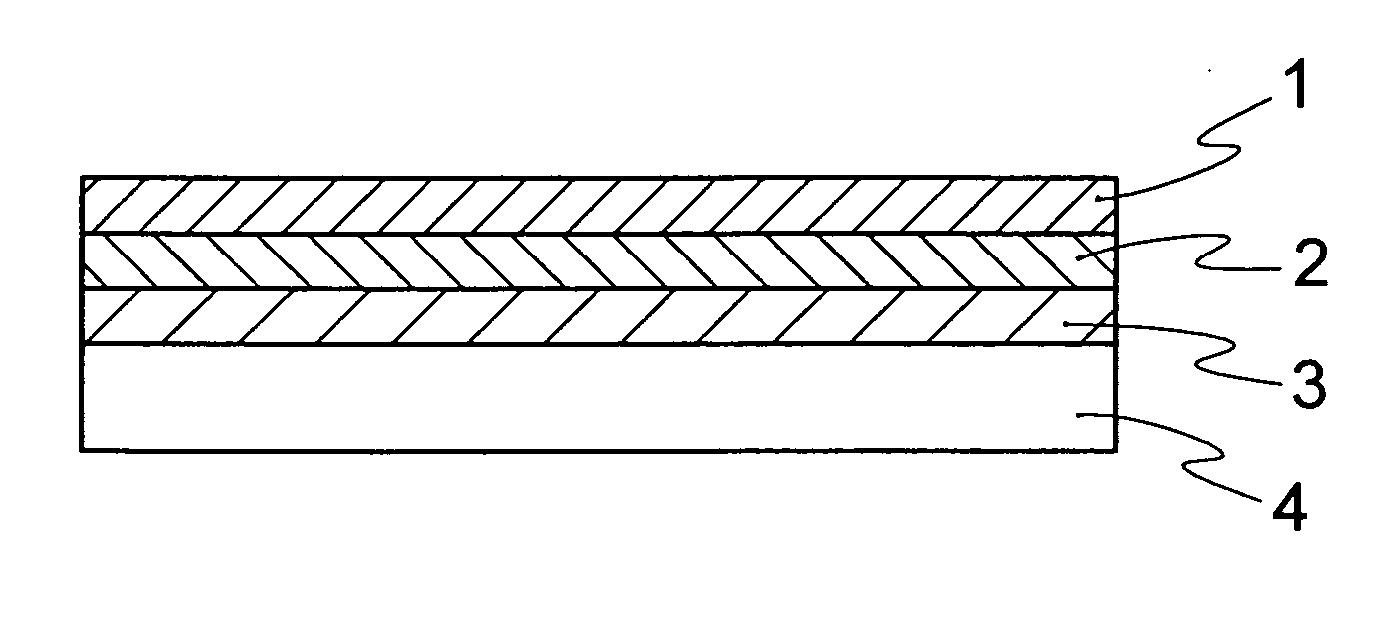
[0147] On one face of a non-thermoplastic polyimide film having thickness of 25 μm prepared in accordance with preparing method A, B, or C, a polyimide film was formed in accordance with for coating a polyamic acid solution prepared by preparing method X or Y. The thickness of a thermoplastic polyimide layer was 3 μm.
[0148] Next, nickel was sputtered for 1 minute on the thermoplastic polyimide layer, and a nickel film having thickness of 6 nm was formed. Copper was continuously sputtered for 9 minutes, a copper film having thickness of 100 nm was formed, and a laminate comprised metal layer / a polyimide film layer was obtained. On the obtained sputtered film, a copper layer having thickness of 18 μm was formed in accordance with an electroplating method. An adhesion strength of this laminate at a normal temperature, an adhesion strength after pressure cooker test, and a de-smear resistance were measured. The measurement result is shown in Table 2.
TABLE 2AdhesionPolyimidestrengthpr...
examples 7 to 14
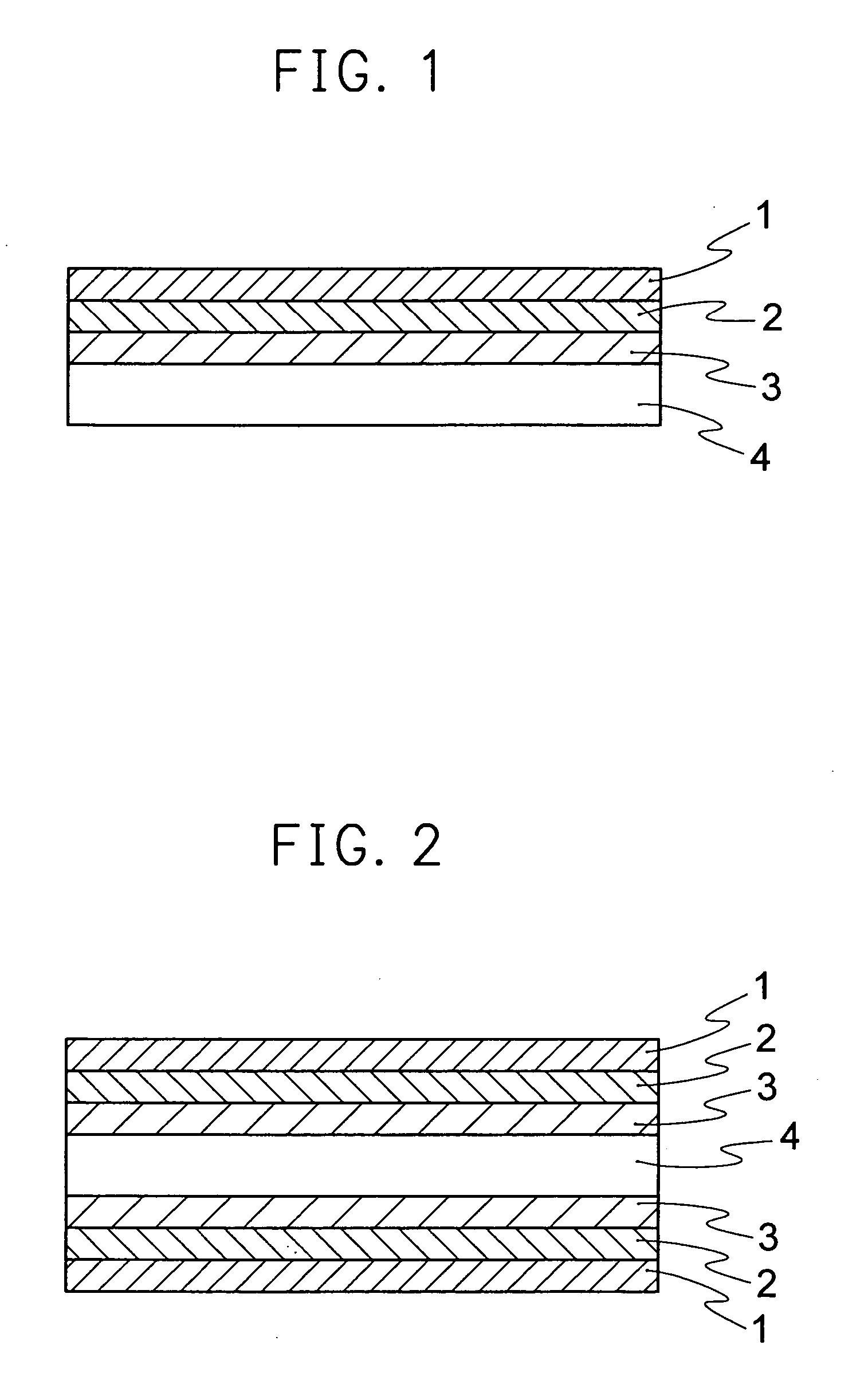
[0150] A sample having formed thereon a thermoplastic polyimide layer having different thickness was produced in accordance with a method of coating a polyamic acid solution prepared by preparing method Y on both faces of a thermoplastic polyimide film having thickness of 25 μm prepared in accordance with preparing method C. On this film, a nickel film having thickness of 6 nm was formed by sputtering nickel for 1 minute. Copper was continuously sputtering for 9 minutes, a copper film having thickness of 100 nm was formed, and a laminate layer consisiting of a metal layer / a polyimide film layer was obtained. By using the thus obtained sputtered film as a feeding layer, a copper layer having thickness of 18 μm was formed in accordance with an electroplating method. An adhesion strength of the obtained laminate at a room temperature; an adhesion strength after pressure cooker test; a de-smear resistance; and a thermal expansion coefficient were measured. The measurement result is show...
PUM
| Property | Measurement | Unit |
|---|---|---|
| Temperature | aaaaa | aaaaa |
| Thickness | aaaaa | aaaaa |
| Thickness | aaaaa | aaaaa |
Abstract
Description
Claims
Application Information