Reflective optical element and EUV lithography appliance

a technology of optical elements and lithography equipment, applied in the field of refractive optical elements, can solve the problems of substantial reflection loss of functional optical surfaces, inability to prevent hydrocarbons and/or other carbon compounds from being inside the appliance, and carbon-containing contamination films on the optical elements, so as to reduce the deposition of contamination on the protective layer system

Inactive Publication Date: 2006-03-30
CARL ZEISS SMT GMBH
View PDF0 Cites 26 Cited by
  • Summary
  • Abstract
  • Description
  • Claims
  • Application Information

AI Technical Summary

Benefits of technology

[0023] In another preferred embodiment, the protective layer system ends toward the vacuum with a layer of a material that is inert to energy injection, that is, to bombardment with EUV protons or to external electric fields. This decreases the probability of spontaneous electron emission, which in turn might split apart the residual gases into reactive cleavage products. Hence, the deposition of contamination on the protective layer system is further reduced. One can influence the inertia to external electromagnetic fields, for example, by giving the surface the lowest possible relief and / or using materials that have a large gap between the valency band and the conduction band. Especially preferred for this are the materials Nb, BN, B4C, Y, amorphous carbon, Si3N4, SiC, as well as silicon dioxide in various stoichiometric relations. The silicon dioxide can be in the amorphous or polycrystalline, or possibly even the crystalline state.

Problems solved by technology

Although EUV lithography appliances have a vacuum or a residual gas atmosphere in their interior, it is not entirely possible to prevent hydrocarbons and / or other carbon compounds from being inside the appliance.
These carbon compounds are split apart by the extreme ultraviolet radiation or by secondary electrons, resulting in the depositing of a carbon-containing contamination film on the optical elements.
This contamination with carbon compounds leads to substantial reflection losses of the functional optical surfaces, which can have a considerable influence on the economic effectiveness of the EUV lithography process.
The contamination leads not only to reflectivity losses, but also to imaging errors, which in the worst case make an imaging impossible.
These significantly increase the operating costs.
But the cleaning cycles not only increase the down time, but also entail the risk of worsening of the homogeneity of the layer thickness of the reflective optical elements and the risk of increasing the surface relief, which leads to further reflectivity losses.

Method used


Image

  • Reflective optical element and EUV lithography appliance
  • Reflective optical element and EUV lithography appliance
  • Reflective optical element and EUV lithography appliance

Examples


example 1

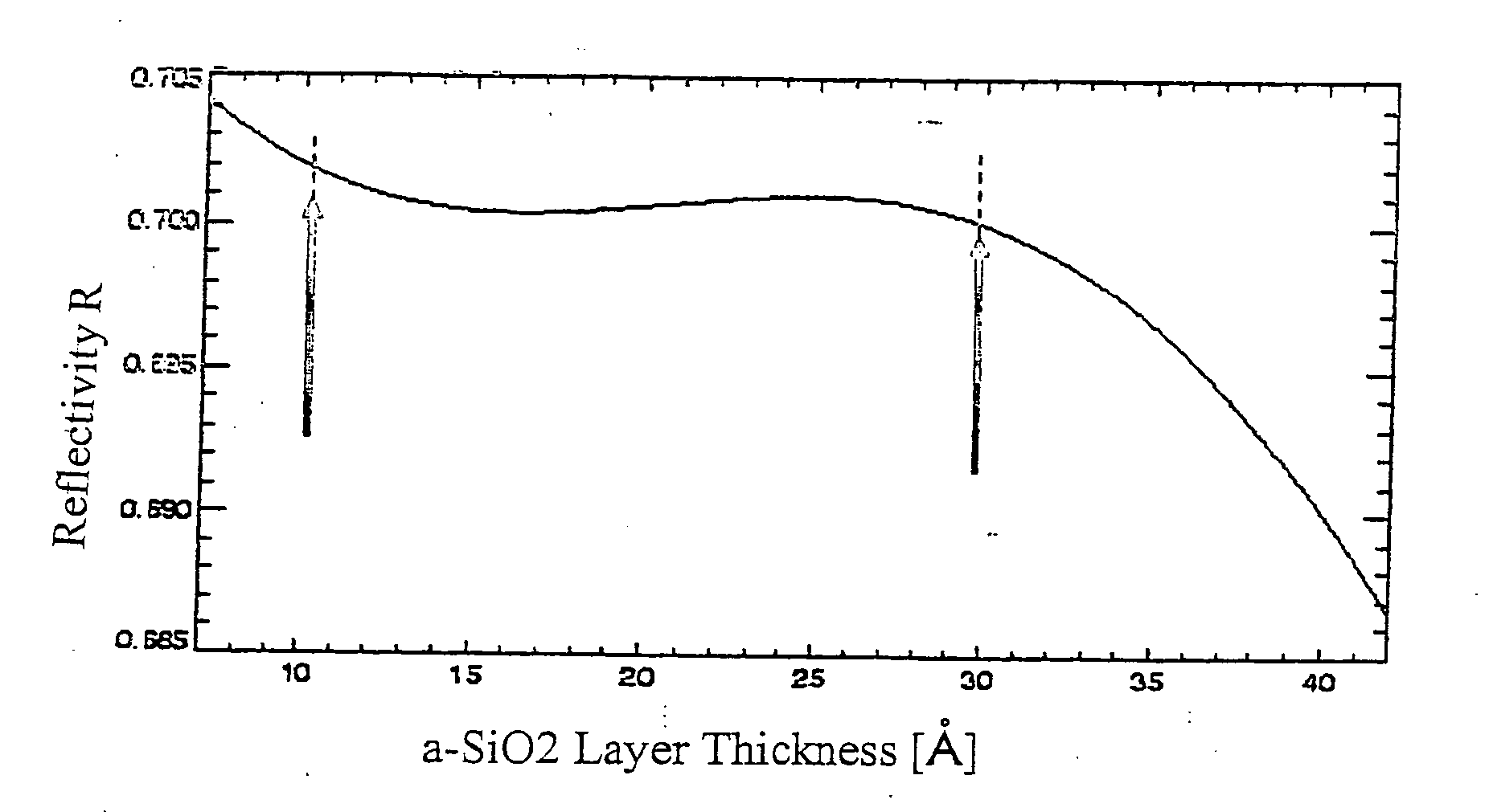
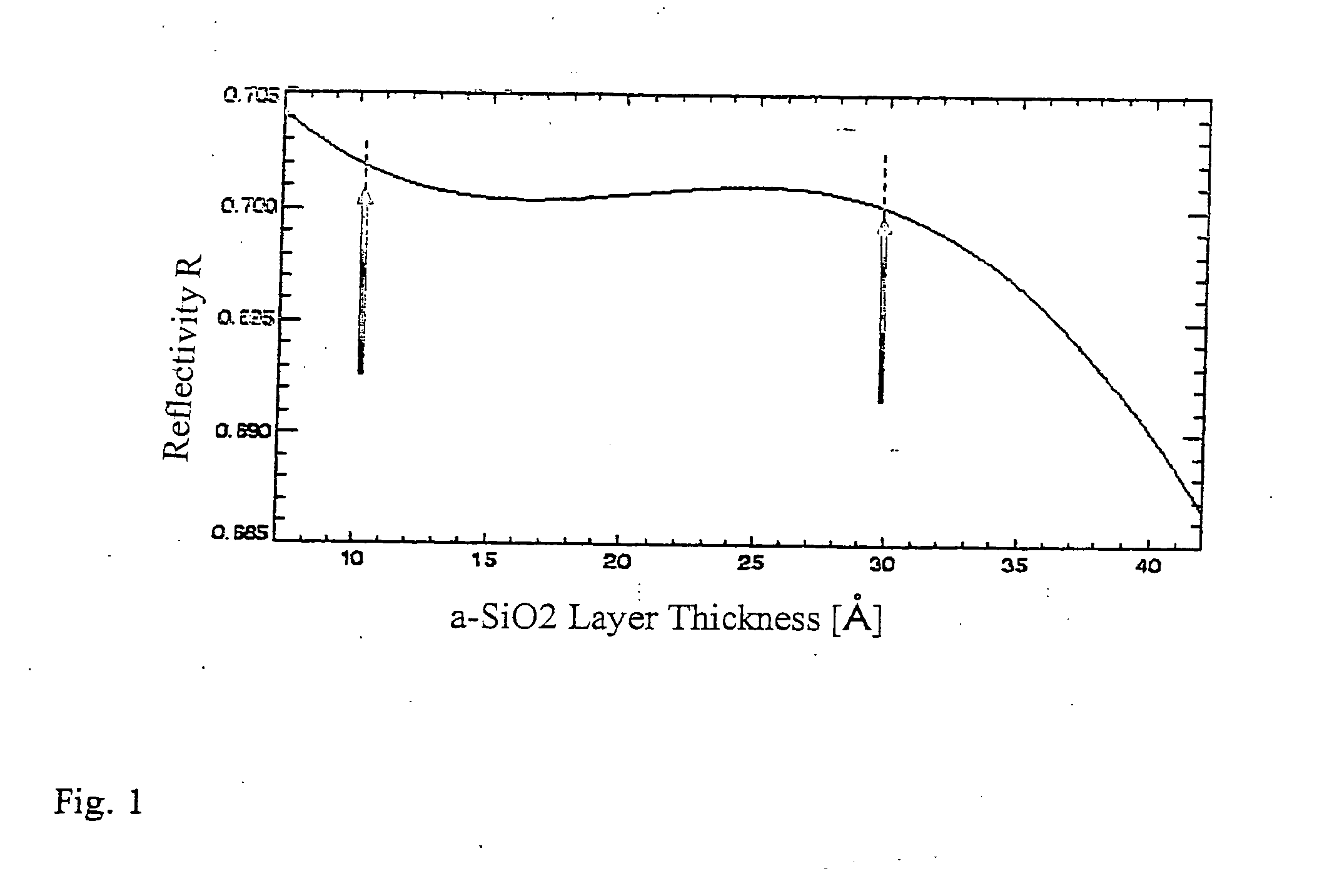
[0030] On a Mo / Si multilayer system located on a substrate of amorphous silicon dioxide, consisting of 50 pairs of 2.76 nm molybdenum and 4.14 nm amorphous silicon (a-SiO2), a three-layer protective layer system is deposited. The protective layer system borders on the uppermost molybdenum layer of the multilayer system with a Y-layer 1.2 nm thick. On the Y-layer is placed a 1.5 nm Y2O3 layer. At the vacuum side, the protective layer system is closed by a 1 nm thick amorphous silicon dioxide layer. The choice of the materials and their thickness is based on the criteria of the invention. In particular, the materials are also selected so as to suppress carbon build-up (Y2O3, a-SiO2) or to be inert to energy injection (Y, a-SiO2).

[0031] Disregarding the interface and surface roughness, one obtains a reflectivity of 70.2% at an operating wavelength of 13.5 nm for an angle of incidence of 0° with the normal to the surface. FIG. 1 shows the reflectivity of the entire reflective optical e...

example 2

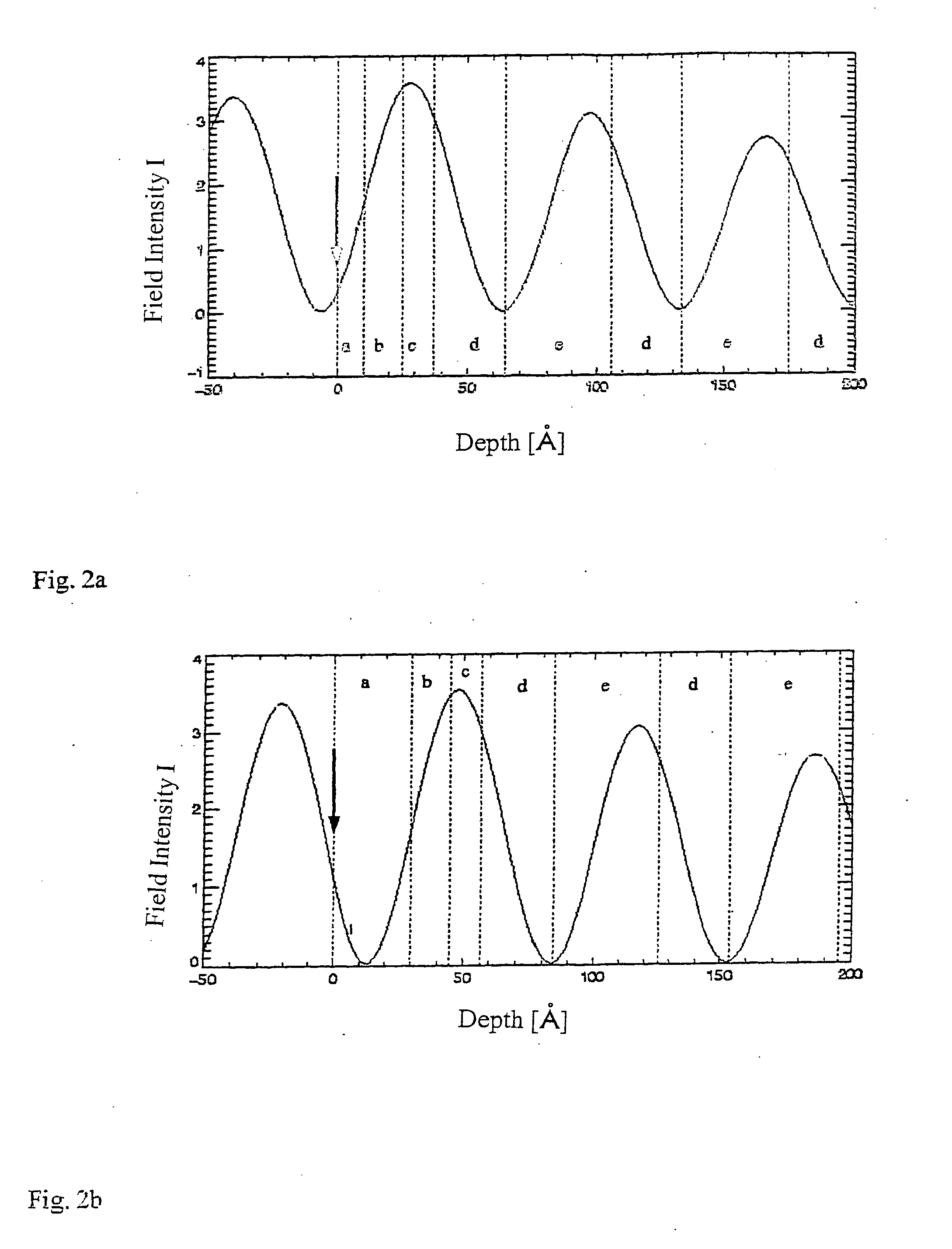
[0037] On a multilayer system of 50 Mo / Si pairs located on an amorphous silicon dioxide substrate, optimized for an operating wavelength of 13.5 nm, a protective layer system of a 2.0 nm thick cerium layer, which adjoins the topmost molybdenum layer of the multilayer system, and a 1.5 nm thick silicon dioxide layer is placed. The minimum of a standing wave produced by reflection on the uncontaminated reflective optical element at operating wavelength λB lies in the vacuum, 0.05λB from its surface. For a maximum reflectivity of 70.9% at an operating wavelength of 13.5 nm and a tolerated reflectivity decrease of 1%, a carbon contamination layer can tolerate a thickness of up to 3.5 nm (see FIG. 5). This reflective optical element as well is suitable for use in an EUV lithography appliance.


PUM

PropertyMeasurementUnit
thicknessaaaaaaaaaa
thicknessaaaaaaaaaa
reflectivityaaaaaaaaaa

Abstract

The invention relates to a reflective optical element and an EUV lithography appliance containing one such element, said appliance displaying a low propensity to contamination. According to the invention, the reflective optical element has a protective layer system consisting of at least one layer. The optical characteristics of the protective layer system are between those of a spacer and an absorber or correspond to those of a spacer. The selection of a material with the smallest possible imaginary part and a real part which is as close to 1 as possible in terms of the refractive index leads to a plateau-type reflectivity course according to the thickness of the protective layer system between two thicknesses d1 and d2. The thickness of the protective layer system is selected in such a way that it is less than d2.

Description

CROSS REFERENCE [0001] This application is a continuation-in-part application of International Application No. PCT / EP2004 / 002014, filed Mar. 1, 2004 and published as WO 2004 / 079753 on Sep. 16, 2004, which claims the priority to German Application No. 103 09 084.3, filed Mar. 3, 2003.FIELD OF THE INVENTION [0002] The invention concerns a reflective optical element for the EUV and soft X-ray wavelength region, having a multilayer system and a protective layer system, wherein the side of the multilayer system facing the protective layer system terminates in an absorber layer. Furthermore, the invention concerns an EUV lithography appliance with a reflective optical element of this kind. BACKGROUND OF THE INVENTION [0003] Multilayers are composed of periodic repetitions, and in the most simple case a period consists of two layers. The one layer material should consist of a so-called spacer material, while the other layer material should consist of a so-called absorber material. Spacer m...

Claims


Application Information

Patent Timeline
Patent Type & Authority Applications(United States)
IPC IPC(8): F21V9/04G02B1/10G03F7/20G21K1/06
CPCB82Y10/00G03F7/70916G03F7/70958G03F7/7015G02B5/0891G02B5/0816G02B5/085G21K1/062
Inventor TRENKLER, JOHANNMANN, HANS-JURGENNOTHELFER, UDO
Owner CARL ZEISS SMT GMBH
Why Eureka
Try Eureka