Method of fabricating an epitaxially grown layer

a technology of epitaxial growth and epitaxial growth, which is applied in the direction of polycrystalline material growth, crystal growth process, after-treatment details, etc., can solve the problems of not being able to fabricate substrates from gallium nitride (gan) ingots on an industrial scale, and existing methods are not suitable for fabricating gallium nitride (gan) ingots. , to achieve the effect of reducing the thickness of the bonded nucleation substra

Active Publication Date: 2006-04-13
S O I TEC SILICON ON INSULATOR THECHNOLOGIES
View PDF59 Cites 73 Cited by
  • Summary
  • Abstract
  • Description
  • Claims
  • Application Information

AI Technical Summary

Benefits of technology

[0030] Preferably, the remainder portion is maintained in contact with, and more preferably engaged against, the detached support portion during the growing of the epitaxial layer. This contact or engagement can help support and stabilize the composite wafer that is thus formed, during the growth of the epitaxial layer. Sufficient strength is provided by these engaged portions to effect the support and stabilization, such as by providing a sufficient thickness to the support substrate.
[0031] In the preferred embodiment, the nucleation portion is transferred by providing a region of weakness within a nucleation substrate to divide the nucleation substrate into and define the nucleation portion and a nucleation substrate remainder portion, which are disp

Problems solved by technology

However, not all of those materials can be obtained by pulling ingots of high crystalline quality.
Further, it is not always possible to fabricate substrates from such ingots because the costs are too high or the method is too difficult to implement.
Thus, for example, existing methods are not suitable for fabricating gallium nitride (GaN) ingots on an industrial scale.
153-158, describes a method of growing a monocrystalline GaN ingot in the liquid phase at a pressure of 12 to 20 kbars (12 to 20×108 Pascals (Pa)) and at a temperature in the range 1400° C. to 1700° C. However, those conditions are difficult to implement under mass production conditions.
Further, they can only produce crystals with a maximum diameter of 18 millimeters (mm).
Other research teams have also worked on a method of growing an ingot in the liquid phase at reduced pressure (less than 2 bars (2×10⁵ Pa)) and at a temperature of 1000° C. The diameter of the crystals obtained is larger, close to 50 mm, but the crystalline quality obtained is not as good as with the above-mentioned technique.
The fabrication conditions employed are a pressure of less than 1 bar (105 Pa) and a temperature of 1000° C. to 1200° C. The crystalline quality obtained is very high, but the crystal size is 3 mm, which is clearly insufficient for the envisaged applications.
Thus, the market currently offers no monocrystalline gallium nitride in the bulk form, of high quality, of a sufficient diameter, and at a reasonable price.
The main drawback of that technique is that the material constituting the support and that deposited by epitaxy general

Method used


Image

  • Method of fabricating an epitaxially grown layer
  • Method of fabricating an epitaxially grown layer
  • Method of fabricating an epitaxially grown layer

Examples


example 1

Production of a Thick Epitaxially Grown Gallium Nitride Layer

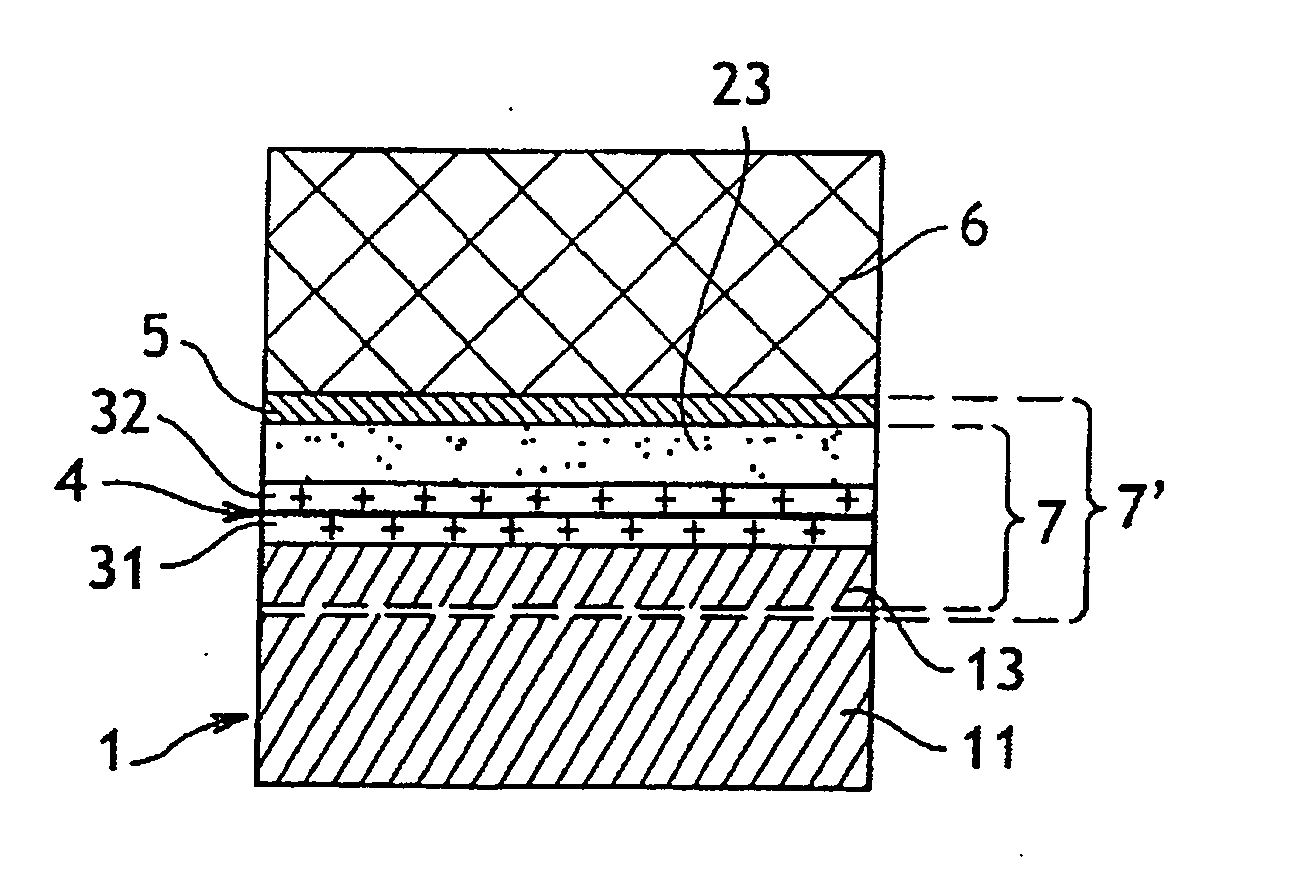
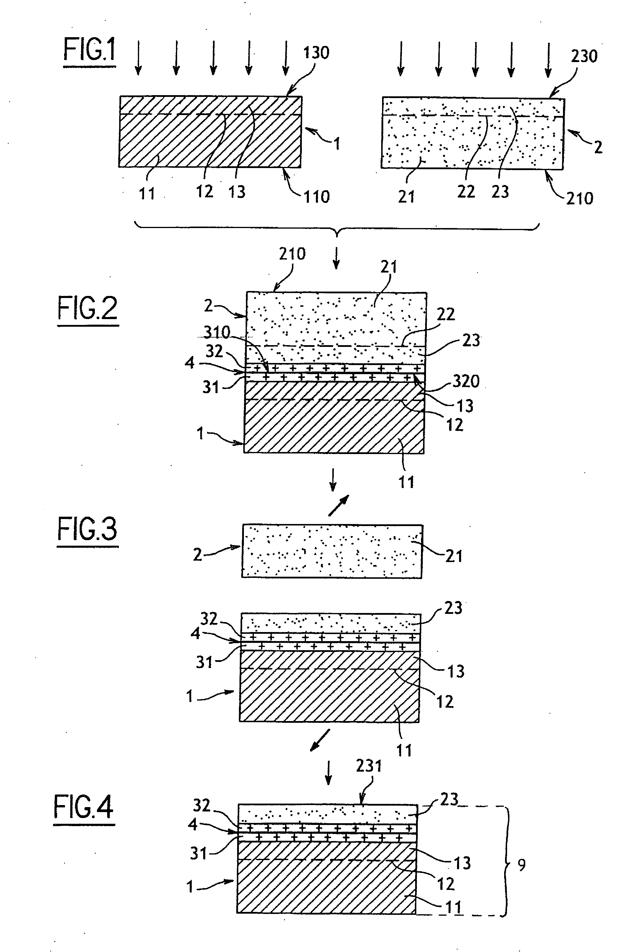
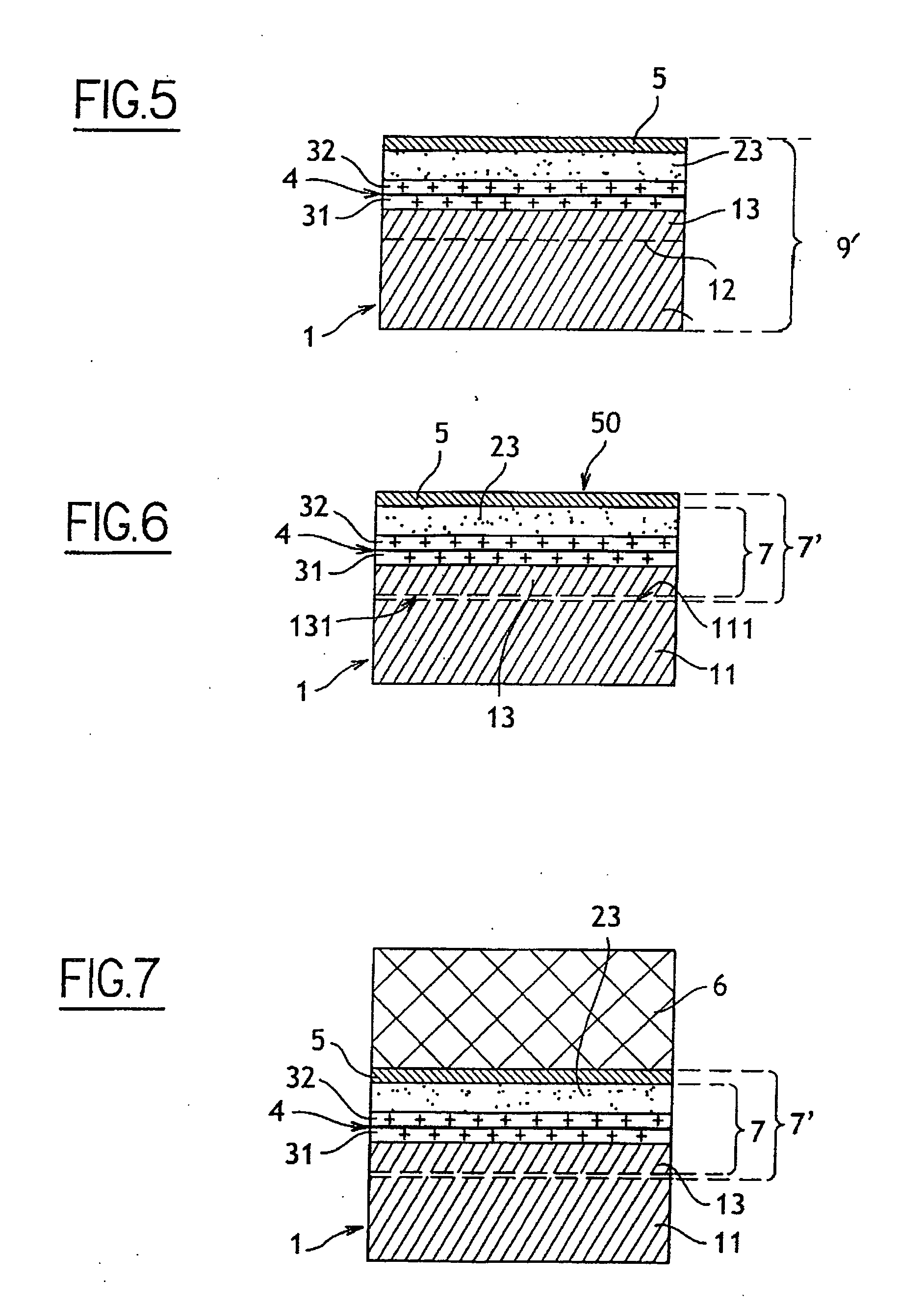
[0133] Hydrogen was implanted into a [111] silicon nucleation substrate 2 through a silicon oxide layer 32 obtained by thermal oxidation.

[0134] Hydrogen was also implanted onto a support substrate 1 formed from polycrystalline silicon carbide (SiC) through a layer of silicon oxide 31 obtained by deposition.

[0135] The implantation conditions for the silicon nucleation substrate 2 were an energy of 120 kilo electron-volts (keV) and a dose of 5×10¹⁶ H+ / cm2, and for the SiC support substrate 1, the energy was 95 keV and the dose was 6×10¹⁶ H+ / cm2.

[0136] The silicon oxide layers 31 and 32 underwent chemico-mechanical polishing, CMP, to activate them and encourage their bonding by molecular bonding.

[0137] The remainder 21 of the [111] silicon layer was then detached by annealing at a temperature of 500° C. for two hours. It should be noted that the thermal budget applied to ensure detachment in the silicon was less than tha...

example 2

Production of a Thick Epitaxially Grown Layer of Monocrystalline Cubic Silicon Carbide

[0142] Hydrogen was implanted into a monocrystalline [001] silicon nucleation substrate 2 through a silicon oxide layer 32 obtained by thermal oxidation.

[0143] Hydrogen was also implanted onto a support substrate 1 formed from polycrystalline silicon carbide (SiC) through a layer of silicon oxide 31 obtained by deposition.

[0144] The implantation conditions for the silicon nucleation substrate 2 were an energy of 120 keV and a dose of 5×10¹⁶ H+ / cm2, and for the SiC support substrate 1, the energy was 95 keV and the dose was 6×10¹⁶ H+ / cm2.

[0145] The silicon oxide layers 31 and 32 underwent chemico-mechanical polishing (CMP) to activate them and to boost bonding by molecular bonding.

[0146] The remainder 21 from the [001] silicon layer was then detached by annealing at a temperature of 500° C. for two hours. It should be noted that the thermal budget applied to ensure detachment in the silicon was...


PUM


Abstract

A method of forming an epitaxially grown layer, preferably by providing a region of weakness in a support substrate and transferring a nucleation portion to the support substrate by bonding. A remainder portion of the support substrate is detached at the region of weakness and an epitaxial layer is grown on the nucleation portion. The remainder portion is separated or otherwise removed from the support portion.

Description

CROSS-REFERENCE TO RELATED APPLICATIONS [0001] This application is a continuation-in-part of PCT Patent Application No. PCT / EP04 / 07578 filed Jul. 7, 2004, the entire content of which is hereby incorporated herein by reference thereto.FIELD OF THE INVENTION [0002] The present invention relates to a method of fabricating an epitaxially grown layer, such as for applications in the fields of optics, optoelectronics, or electronics. BACKGROUND OF THE INVENTION [0003] Certain materials, for example silicon, having properties that are particularly interesting in the fields mentioned above, can be obtained in large quantities and with excellent quality using ingot pulling techniques that are well known to the skilled person. [0004] The ingots obtained are then readily sliced into wafers which, after a large number of processing steps, become substrates that are used to produce integrated circuits, for example. [0005] Other materials such as gallium arsenide, gallium nitride, indium phosphid...

Claims


Application Information

Patent Timeline
IPC IPC(8): H01L29/04H01L21/36C30B25/18C30B33/00H01L21/762
CPCC30B25/18C30B33/00H01L21/76254Y10S438/928Y10S438/977C30B25/02C30B23/02
Inventor FAURE, BRUCELETERTRE, FABRICE
Owner S O I TEC SILICON ON INSULATOR THECHNOLOGIES
Why Eureka
Try Eureka