

Structure and method for contact pads having an overcoat-protected bondable metal plug over copper-metallized integrated circuits
a technology of integrated circuits and contact pads, which is applied in the direction of semiconductor/solid-state device testing/measurement, semiconductor devices, semiconductor/solid-state device details, etc., can solve the problems electrical shorting, and pronounced resistance of aluminum to electromigration becoming a serious obstacle, so as to reduce the risk of aluminum smearing or scratching and electrical shorting, and facilitate the shrinking of the pitch of the contact pads
- Summary
- Abstract
- Description
- Claims
- Application Information
AI Technical Summary
Benefits of technology
Problems solved by technology
Method used
Image

Examples
Embodiment Construction
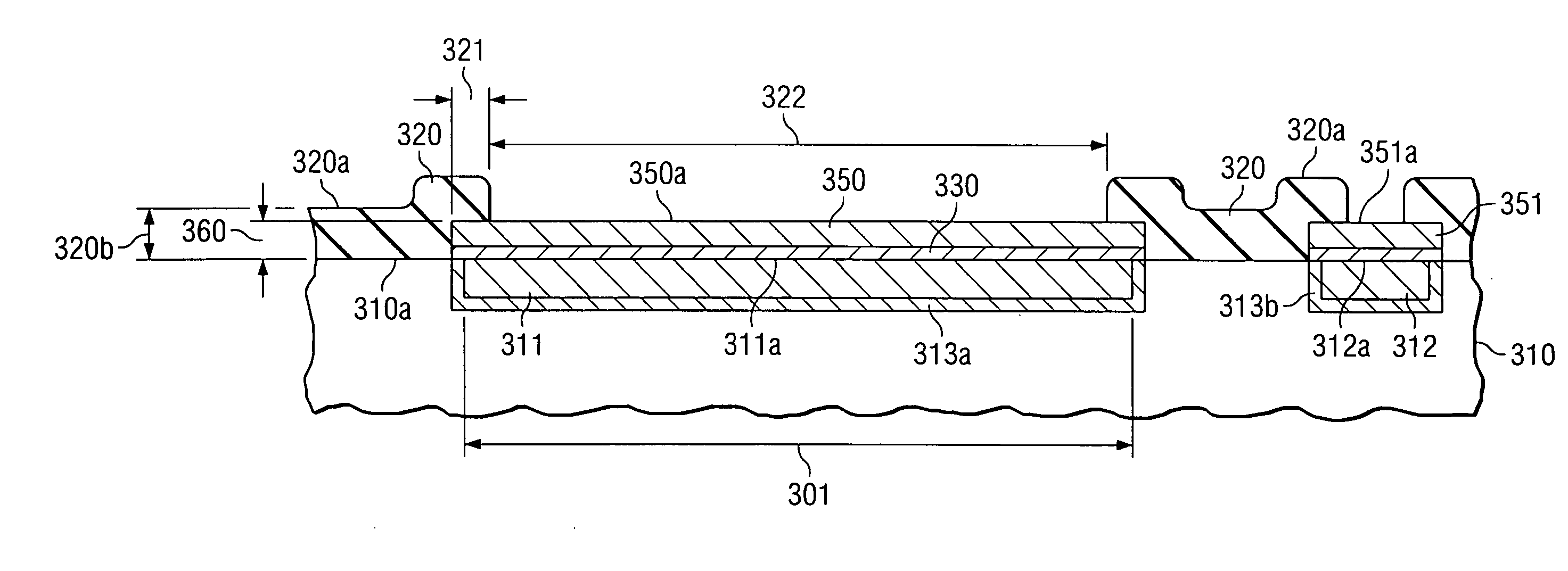
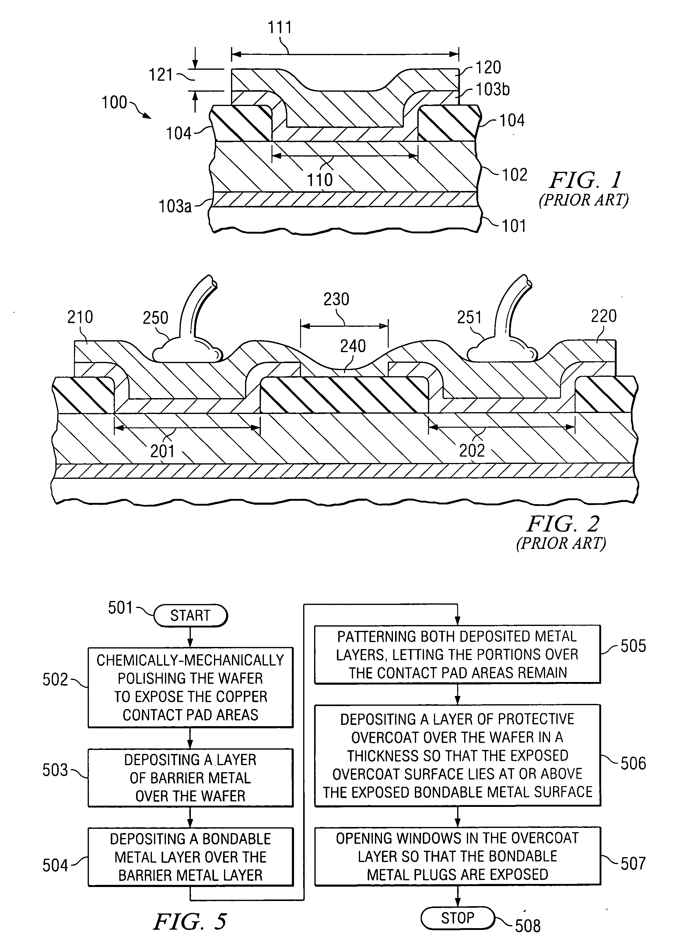
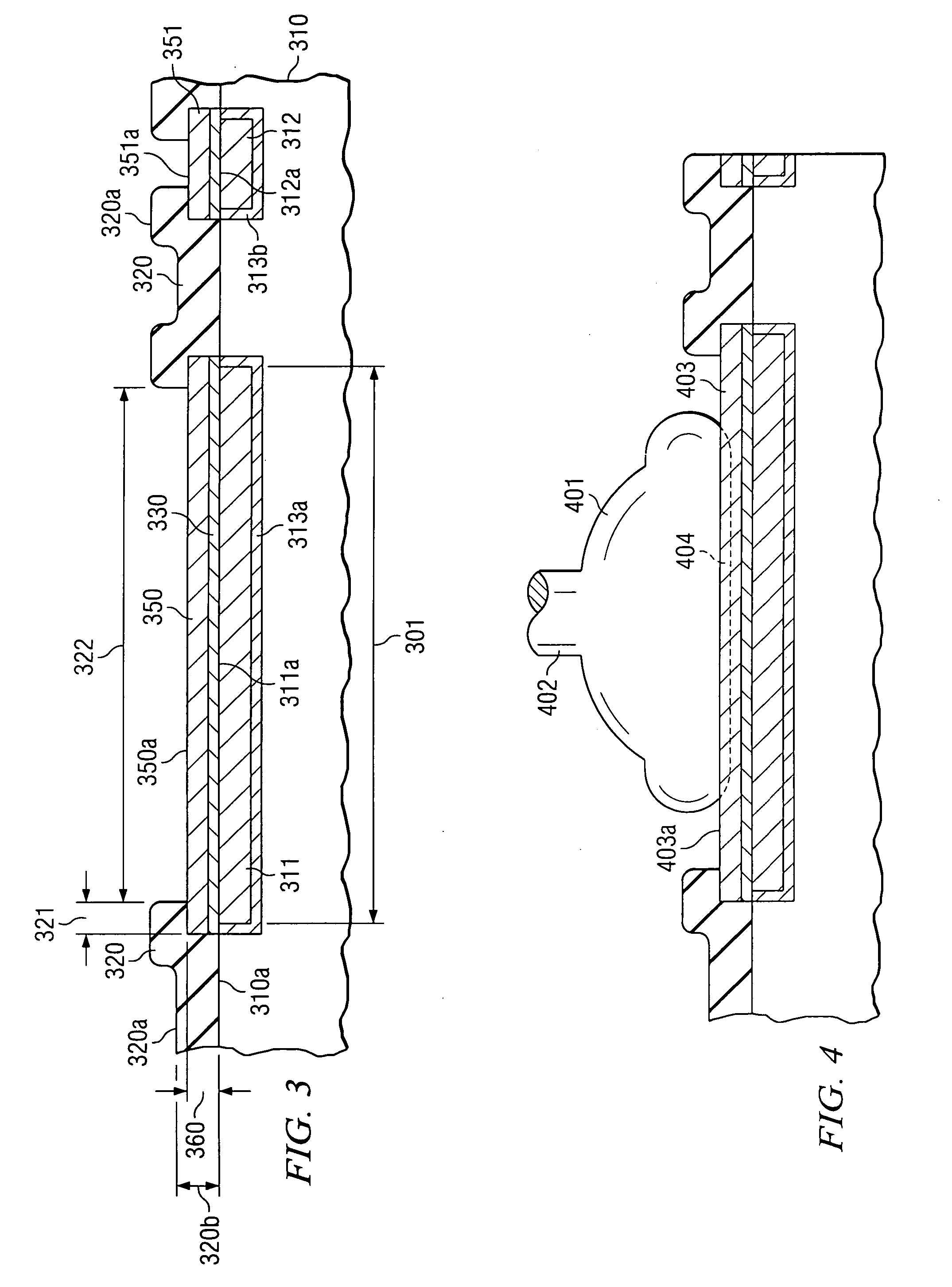
[0017] The technical advantages offered by the invention can be best appreciated by comparing an embodiment of the invention with the conventional method of wire-bonding a contact pad of an integrated circuit (IC) chip, which uses copper as interconnecting metal. An example of a conventional structure is depicted in FIG. 1. In the schematic cross section of an IC contact pad generally designated 100, 101 is an intra-level dielectric, which may consist of silicon dioxide, a low-k dielectric, or any other suitable insulator customarily used in ICs. 102 represents the top level IC copper metallization (thickness typically between 200 and 500 nm, contained by barrier layers 103a and 103b (typically tantalum nitride, typically 10 to 30 nm thick) from diffusing into other IC materials. In the essentially moisture-impermeable overcoat layer 104 (typically between 500 to 1000 nm of silicon nitride, silicon oxynitride, or silicon dioxide, single-layered or multi-layered) is contact window 11...
PUM
| Property | Measurement | Unit |
|---|---|---|
| thickness | aaaaa | aaaaa |
| thickness | aaaaa | aaaaa |
| width | aaaaa | aaaaa |
Abstract
Description
Claims
Application Information