Method for patterning carbon nanotube coating and carbon nanotube wiring

a technology of carbon nanotubes and wiring lines, which is applied in the manufacture of electrode systems, nanoinformatics, electric discharge tubes/lamps, etc., can solve the problems of forming a layer that practically blocks light, the wiring lines formed by the above methods are not well-received, and the installation and maintenance of such instruments are expensiv

Inactive Publication Date: 2006-05-25
ARTHUR DAVID J +1
View PDF17 Cites 74 Cited by
  • Summary
  • Abstract
  • Description
  • Claims
  • Application Information

AI Technical Summary

Benefits of technology

[0013] This invention overcomes the problems and disadvantages associated with current metal-based and silicon-based wiring technologies and provides new wiring methods that utilize carbon nanotube film to form a wiring line and an electrode.

Problems solved by technology

Whatever the vacuum level is, the installation and maintenance of such instruments are expensive.
Furthermore, all of the wiring lines formed by above methods do not transmit light well with an exception of those made of inorganic electrode materials such as indium tin oxide (ITO).
Extremely thin metal films may be translucent, but stacking of such films results in forming of a layer that practically blocks light.
A transparent ITO film may be formed relying on the high level vacuum instruments, but is not flexible due to its inorganic nature.
Furthermore, the supply of indium is limited.
Though these fabrication methods are inexpensive, it is not possible to make compact device, such as a semiconductor device, relying on these methods.
Furthermore, the wiring lines made by these methods are not transparent.
Accordingly, the wiring structures made by these methods are not applicable to devices that require fine patterning of transparent conductive film, such as electroluminescent display device and liquid crystal display device.
However, this ITO filled system cannot match the electrical conductivity of a continuous ITO film.
Although they are still at a development stage and yet to reach the conduction level of a ITO film, the presence of dopants is expected to have an adverse effect on controlling the conductive properties, and may not be compatible with device miniaturization.
However, there have been no report in the art on a method for patterning the film made of carbon nanotubes.

Method used


Image

  • Method for patterning carbon nanotube coating and carbon nanotube wiring
  • Method for patterning carbon nanotube coating and carbon nanotube wiring
  • Method for patterning carbon nanotube coating and carbon nanotube wiring

Examples


example 1

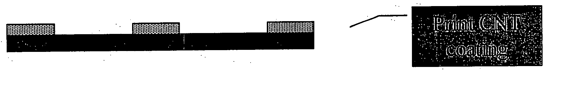
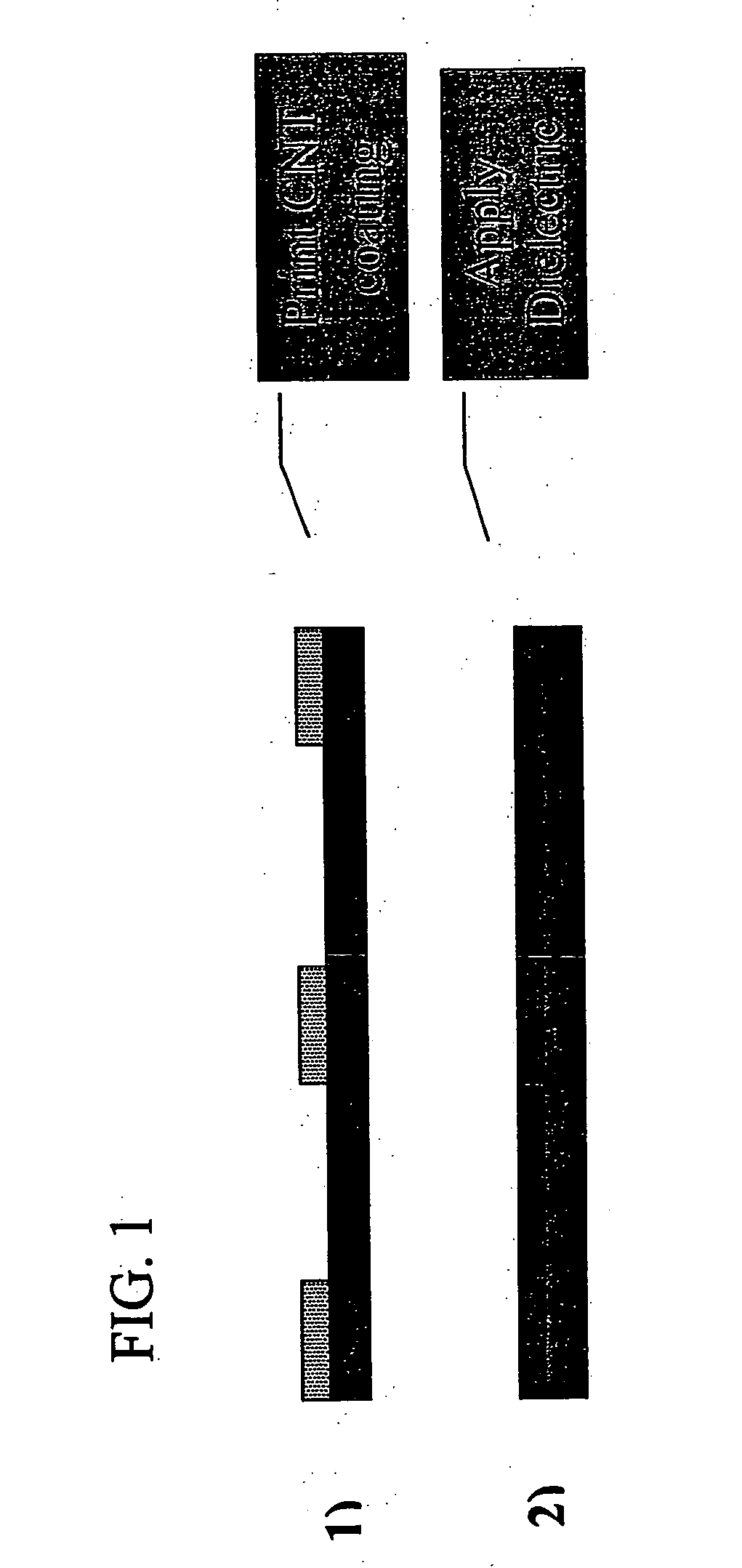
[0042] First, as purchased SWNTs are purified by process steps including acid reflex, water rinsing, centrifuge and microfiltration. Then, the purified SWNTs are mixed into a solution of isopropyl alcohol (IPA) and water to form a carbon nanotube coating solution. The SWNT solids content is in the range of 10 to 100 ppm by weight. The weight ratio of IPA to water is in the range of 1:3 to 3:1, depending on the drying rate desired for the coating. Once a reasonably stable dispersion has been achieved, the viscosity of the SWNT dispersion is increased by adding a sufficient amount of a polyacrylic acid, a viscosity modifying agent (Acrysol ASE 75, available from Rohm & Haas), to provide a coating composition having a viscosity suitable for gravure coating, (e.g., approximately 1000 cP). The carbon nanotube coating solution is printed onto a clear plastic film (e.g., polyethersulfone) using a patterned gravure roll. The IPA / water and viscosity modifier are then removed by heating, leav...

example 2

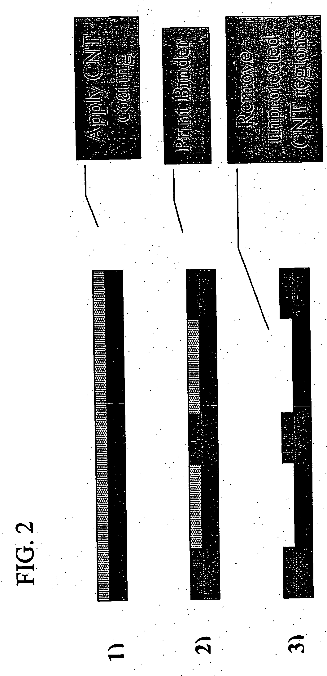
[0043] First, as purchased SWNTs are purified by process steps including acid reflex, water rinsing, centrifuge and microfiltration. Then, the purified SWNTs are mixed into a solution of isopropyl alcohol (IPA) and water to form a carbon nanotube coating solution. The SWNT solids content is in the range of 10 to 100 ppm by weight. The weight ratio of IPA to water is in the range of 1:3 to 3:1, depending on the drying rate desired for the coating. The SWNT coating is applied to a clear plastic film (e.g., polyester film such as PET or PEN film from Dupont Teijin Films) using an atomized spraying technique. The substrate is heated to 60° C. to increase drying rate of the IPA / water. A sufficient thickness of the consolidated carbon nanotubes is applied to achieve the desired electrical resistance (e.g., 500 ohms / square). Then, a binder coating such as acrylic resin dissolved in ethyl acetate is printed using a screen printing technique. The binder coating permeates selected regions of ...

example 3

[0044] First, as purchased SWNTs are purified by process steps including acid reflex, water rinsing, centrifuge and microfiltration Then, the purified SWNTs are mixed into a solution of isopropyl alcohol (IPA) and water to form a carbon nanotube coating solution. The SWNT solids content is in the range of 10 to 100 ppm by weight. The weight ratio of IPA to water is in the range of 1:3 to 3:1, depending on the drying rate desired for the coating. The SWNT coating is applied to a glass substrate using an atomized spraying technique. The substrate is heated to 60° C. to increase drying rate of the IPA / water. A sufficient thickness of consolidated carbon nanotubes is applied to achieve the desired electrical resistance (e.g., 500 ohms / square). Then, a photo definable polyimide binder such as HD-4000 Series from HD Microsystems is applied to the consolidated carbon nanotube film using a Meyer rod coating technique. The photoresist permeates the carbon nanotube film. A predetermined wirin...


PUM

PropertyMeasurementUnit
outer diameteraaaaaaaaaa
light transmittanceaaaaaaaaaa
total light transmittanceaaaaaaaaaa

Abstract

A method for making a nanocomposite electrode or circuit pattern includes forming a continuous carbon nanotube layer impregnated with a binder and patterning the binder resin using various printing or photo imaging techniques. An alternative method includes patterning the carbon nanotube layer using various printing or imaging techniques and subsequently applying a continuous coating of binder resin to the patterned carbon nanotube layer. Articles made from these patterned nanocomposite coatings include transparent electrodes and circuits for flat panel displays, photovoltaics, touch screens, electroluminescent lamps, and EMI shielding.

Description

REFERENCE TO RELATED APPLICATIONS [0001] This invention claims priority to U.S. Provisional Application No. 60 / 381,809 entitled NT Mixtures, and U.S. Provisional Application No. 60 / 381,810 entitled Patterning NT-Based Coatings, both of which were filed on May 21, 2002.BACKGROUND [0002] 1. Filed of the Invention [0003] This invention is directed to methods for patterning carbon nanotube coatings and carbon nanotube wiring made by the methods. [0004] 2. Description of the Background [0005] Current electronic devices, including semiconductor-based devices as well as wiring circuits of larger scale, rely on conventional wiring technologies that use metal wiring lines or high impurity regions formed in a semiconductor substrate. Semiconductor-based devices have metal wiring layers that are formed on the semiconductor substrate and interconnect device elements formed on the surface of the semiconductor substrate. The metal layers themselves are often interconnected by via holes piercing t...

Claims


Application Information

Patent Timeline
Patent Type & Authority Applications(United States)
IPC IPC(8): H01J9/12C01B31/02H01L51/30H01L51/40H05K1/09H05K3/02H05K3/04
CPCB82Y10/00H01J1/304H01J2201/30469H01L51/0018H01L51/0048H05K1/095H05K3/02H05K3/046H05K3/12H05K2201/026H05K2201/0323H05K2203/0514H05K2203/0522H05K2203/1147Y10S977/89Y02E10/549H10K71/233H10K85/221
Inventor ARTHUR, DAVID J.GLATKOWSKI, PAUL J.
Owner ARTHUR DAVID J
Why Eureka
Try Eureka