Electroric device, integrated circuit, and method of manufacturing the same

a technology of integrated circuits and electromechanical devices, applied in thermoelectric devices, nanostructure manufacturing, nanoinformatics, etc., can solve the problems of insufficient integration techniques, reduced probability of occurrence, and very thin fibrous material of carbon nanotubes, etc., to achieve high availability, stably patterned, and high productivity.

Inactive Publication Date: 2006-06-08
FUJIFILM BUSINESS INNOVATION CORP
View PDF7 Cites 39 Cited by
  • Summary
  • Abstract
  • Description
  • Claims
  • Application Information

AI Technical Summary

Benefits of technology

[0071] In the method of manufacturing an electronic device of the present invention, when 3 electrodes are arranged in a carbon nanotube structure having a network structure in which carbon nanotubes are chemically bonded to form cross-linked sites, and one of the electrodes is used as a control electrode, it has been found that not only a single-wall carbon nanotube but also a multi-wall carbon nanotube having high productivity and high availability exhibits characteristics similar to those of a semiconductor device. This carbon nanotube is patterned after it has been structured into a network shape that can be stably patterned. As a result, high density patterning, which has been difficult in a contact state, can be performed without reliance on accidental contact between carbon nanotubes. Therefore, the method of manufacturing an electronic device of the present invention is a manufacturing method which is extremely excellent in productivity as compared to a conventional approach and which is suitable for forming a top-down integrated circuit because an electronic device can be assuredly and effectively obtained with the method of the present invention. The method of manufacturing an electronic device of the present invention provides an extremely revolutionary method for embodying a highly integrated device using a carbon nanotube which has been currently promising.
[0072] As described above, according to the present invention, there can be provided an electronic device and an integrated circuit each having stable electrical characteristics. Furthermore, a uniform electronic device using a carbon nanotube can be produced with extreme efficiency.

Problems solved by technology

However, a carbon nanotube is a very thin fibrous material.
Alternatively, a photo tweezer method or an orientation method by means of an electric field are disclosed, but these methods are not different from the above method in that the connection occurs only by chance, and hence are insufficient as techniques for integration.
In a mere dispersion film, an electrical pulse may occur somewhere if a channel has a large area, but the probability of the occurrence reduces as the channel is thinned, so high density is hardly obtained.
Furthermore, for performing thinning and integration, an excessive nanotube must be cut and removed because a tip of a long carbon nanotube lying off the area may establish a short circuit with other device or wiring.
However, it is extremely difficult to pattern a deposit in a contact state, and carbon nanotubes scatter during an etching operation, so patterning is impossible in fact.
In addition, the deposit is merely in contact, so there arises a drawback in that the resultant device is unstable and the current fluctuates in association with vibration or application of a voltage.
However, contact between carbon nanotubes hardly occurs owing to the presence of the resin, thereby leading to a problem in terms of electrical contact.
In addition, the density of carbon nanotubes reduces owing to the presence of the resin, so the number of electrical paths reduces, thereby making it difficult to use the device as an electronic device.
If a mixing amount of carbon nanotubes is increased to solve this, an amount of binders reduces, with the result that the strength of the dispersion film itself reduces and the same problem as that of the above deposit film occurs.

Method used


Image

  • Electroric device, integrated circuit, and method of manufacturing the same
  • Electroric device, integrated circuit, and method of manufacturing the same
  • Electroric device, integrated circuit, and method of manufacturing the same

Examples


example 1

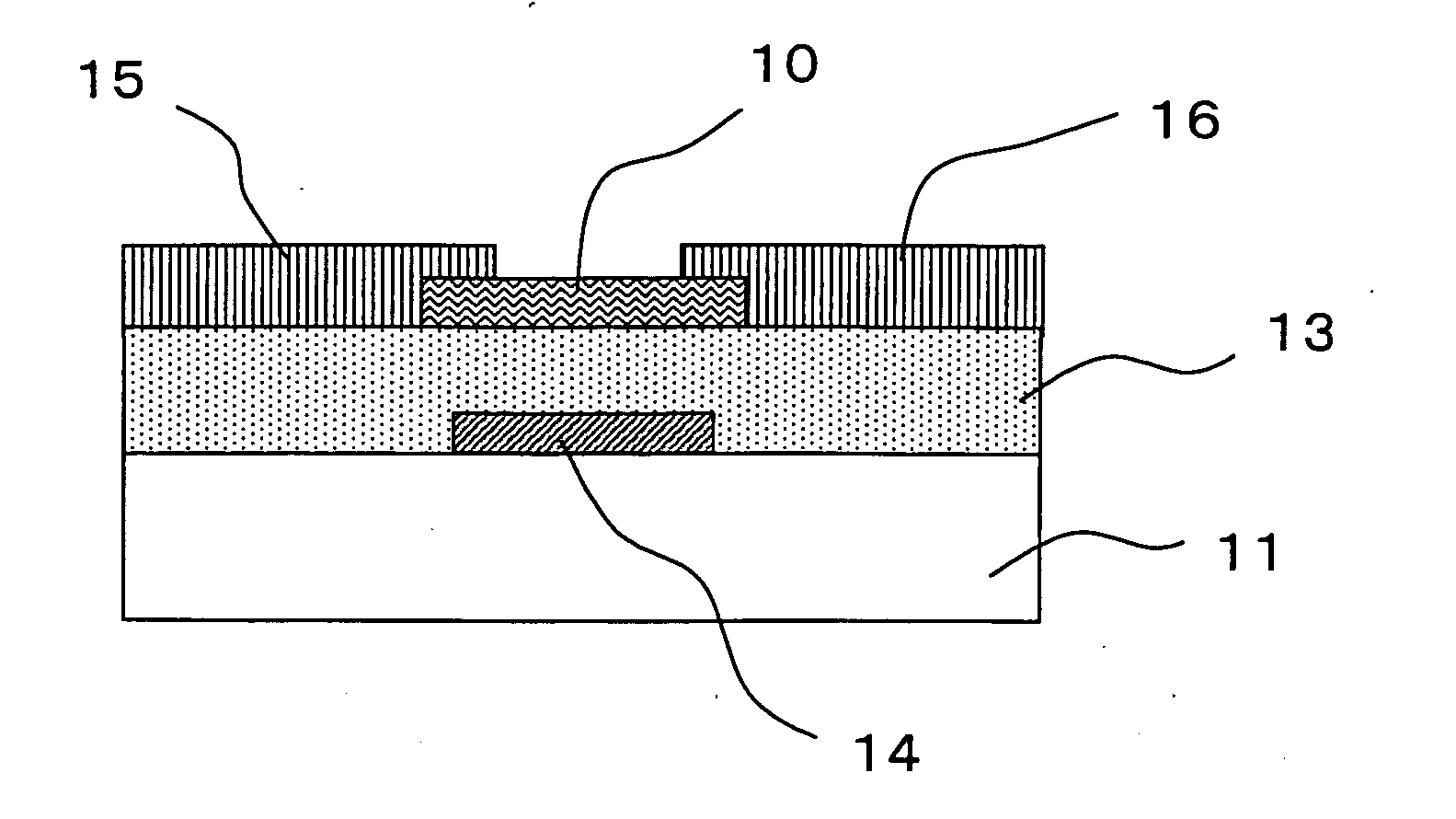
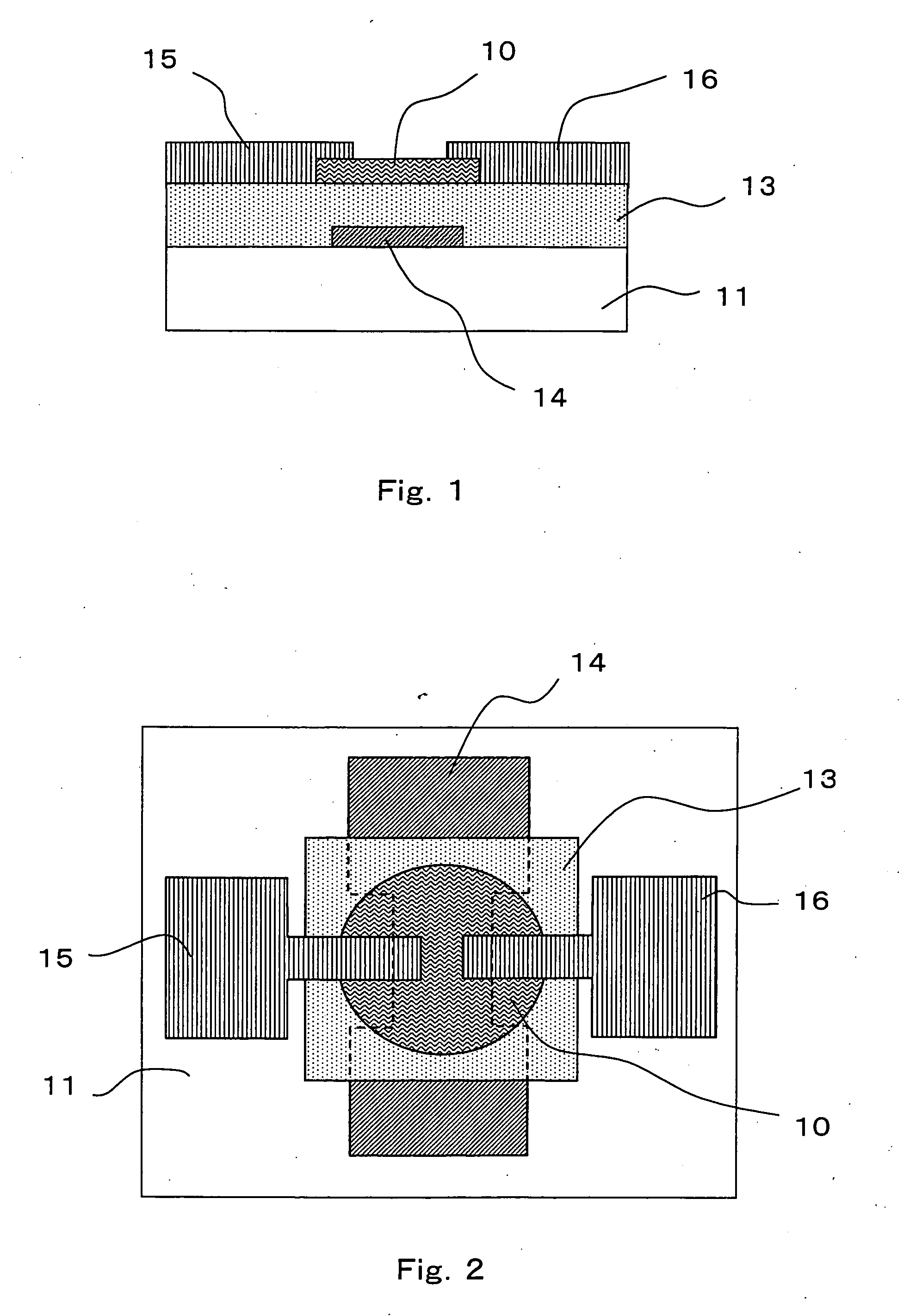
[0277] A MOS-FET carbon nanotube transistor was manufactured through a flow of the method of manufacturing an electronic device shown in FIGS. 4 and 5. It should be noted that reference numerals in FIGS. 4 and 5 may be used in the description of this example.

(A) Applying Step (A-1) Preparation of Cross-Linking Application Solution (Adding Step)

(i) Purification of Single-Wall Carbon Nanotube

[0278] Single-wall carbon nanotube powder (purity 40%, manufactured by Sigma-Aldrich Co.) was sifted through a sieve (125 μm in pore size) in advance to remove a coarse agglomerate. 30 mg of the remainder (having an average diameter of 1.5 nm and an average length of 2 μm) were heated at 450° C. for 15 minutes by using a muffle furnace, and then a carbon substance other than a carbon nanotube was removed. 15 mg of the remaining powder were immersed in 10 ml of a 5-N aqueous solution of hydrochloric acid {prepared by diluting concentrated hydrochloric acid (a 35% aqueous solution, manufactured...

example 2

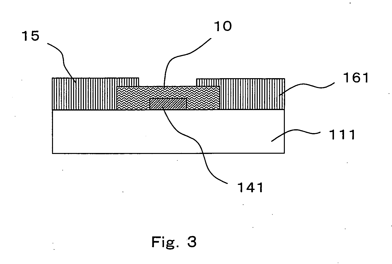
[0308] A MES-FET carbon nanotube field effect transistor shown in FIG. 3 was produced in the same manner as in Example 1 except that the insulating film forming step was omitted. At this time, the gate electrode width and the distance between the source and drain electrodes were set to 500 μm and 1,500 μm, respectively. Then, the field effect transistor was subjected to measurement by means of a parameter analyzer 4156B (manufactured by Agilent Technologies) in the same manner as in Example 1 to confirm a change in electric conductivity between the source and the drain with the gate voltage Vgs. The result confirmed that the current between the source and the drain can be controlled by the gate voltage (FIG. 11).

example 3

[0309] A carbon nanotube structure was formed by using a cross-linking application solution using a multi-wall carbon nanotube, and a MOS-FET carbon nanotube field effect transistor shown in FIG. 1 was produced in the same manner as in Example 1. A method of forming an applied film will be shown below. The other steps were the same as those of Example 1.

(A) Applying Step

(A-1) Preparation of Cross-Linking Application Solution (Addition Step)

(i) Addition of Carboxyl Group . . . Synthesis of Carbon Nanotube Carboxylic Acid

[0310] 30 mg of multi-wall carbon nanotube powder (purity: 90%, average diameter: 30 nm, average length: 3 μm, manufactured by Science Laboratory Inc.) were added to 20 ml of concentrated nitric acid (a 60 mass % aqueous solution, manufactured by KANTO KAGAKU) for reflux at 120° C. for 20 hours to synthesize a carbon nanotube carboxylic acid.

[0311] The temperature of the solution was returned to room temperature and the solution was subjected to centrifugal se...


PUM

PropertyMeasurementUnit
Young's moduliaaaaaaaaaa
diameteraaaaaaaaaa
diameteraaaaaaaaaa

Abstract

The present invention provides an electronic device including a transporting layer which involves a low environmental load and which is excellent in semiconductor characteristics by means of a configuration having, on the surface of a base body, at least a transporting layer constituted by a carbon nanotube structure layer having a network structure in which a plurality of carbon nanotubes mutually cross-link. Also, provided is a method of manufacturing the same.

Description

TECHNICAL FIELD [0001] The present invention relates to an electronic device using a carbon nanotube structure as a transporting layer, an integrated circuit using the electronic device, and a method of manufacturing the same. BACKGROUND ART [0002] Carbon nanotubes (CNTs), with their unique shapes and characteristics, are being considered for various applications. A carbon nanotube has a tubular shape of one-dimensional nature which is obtained by rolling one or more graphene sheets composed of six-membered rings of carbon atoms into a tube. A carbon nanotube which is formed from one graphene sheet is called a single-wall nanotube (SWNT), while a carbon nanotube which is formed from multiple graphene sheets is called a multi-wall nanotube (MWNT). SWNTs are about 1 nm in diameter, while multi-wall carbon nanotubes measure several tens nm in diameter, and both are far thinner than their predecessors, which are called carbon fibers. [0003] One of the characteristics of carbon nanotubes...

Claims


Application Information

Patent Timeline
Patent Type & Authority Applications(United States)
IPC IPC(8): H01L29/08B82B1/00C01B31/02H01L21/336H01L21/338H01L29/06H01L29/66H01L29/786H01L29/812H01L51/00H01L51/05H01L51/30H01L51/40
CPCB82Y10/00B82Y40/00H01L51/0048H01L51/0052H01L51/0512H10K85/221H10K85/615H10K10/462H01L29/66H01L29/06
Inventor HIRAKATA, MASAKIISOZAKI, TAKASHIKISHI, KENTAROSHIGEMATSU, TAISHIWATANABE, MIHOMANABE, CHIKARAANAZAWA, KAZUNORIWATANABE, HIROYUKIOKADA, SHINSUKEOOMA, SHIGEKI
Owner FUJIFILM BUSINESS INNOVATION CORP
Why Eureka
Try Eureka