Vapor deposition of tungsten nitride

a technology of tungsten nitride and vapor deposition, which is applied in the direction of organic compounds without c-metal linkages, instruments, and semiconductor/solid-state device details without c-metal links, etc. it can solve the problems of wf/sub>6/sub>, self-limiting ald reactions, and insufficient uniform thickness of film inside narrow features, etc., to achieve uniform thickness and smooth surfaces. , the effect of high efficiency

Active Publication Date: 2006-06-15
PRESIDENT & FELLOWS OF HARVARD COLLEGE
View PDF4 Cites 241 Cited by
  • Summary
  • Abstract
  • Description
  • Claims
  • Application Information

AI Technical Summary

Benefits of technology

[0008] The present invention provides a highly efficient process for depositing conformal coatings, particularly those containing tungsten, on solid substrates. These coatings comprise tungsten, nitrogen, and optionally, may contain oxygen, silicon, carbon and/or hydrogen...

Problems solved by technology

WNx has been made by reactive sputtering, but the uniformity of film thickness inside narrow features (“step coverage”) is not expected to be adequate for use in future microelectronic devices having narrow features with high aspect ratios.
One particularly important aspect of this process is that the ALD reactions are self-limiting, in that only a certain maximum thickness can form in each cycle, after which no further deposition occurs during that cycle, even if excess reactant is available.
A disadvantage of this process is that WF6 and/or its reaction byproduct, HF, can attack s...

Method used


Image

  • Vapor deposition of tungsten nitride
  • Vapor deposition of tungsten nitride
  • Vapor deposition of tungsten nitride

Examples


example 1

Synthesis of bis(tert-butylimido)bis(dimethylamido) tungsten(VI), (t-BuN)2(Me2N)2W

[0044] 1) To a purple suspension of WCl6 (30.0 g, 75.6 mmol) in toluene (300 mL) a solution of HN(t-Bu)SiMe3 (50 g, 344 mmol) in toluene (65 mL) was added dropwise over a period of 2 h. The suspension was stirred for a total of 24 h. The dark green suspension was filtered through Celite to remove the solid (t-Bu)(Me3Si)NH2Cl and any unreacted WCl6. The dark brown filtrate was dried under vacuum in a warm water bath. 50 mL of hexane was added to the resulting dark brown solid and stirred in order to dissolve some impurities. The brown suspension was cooled in the freezer for overnight, and then the dark brown supernatant solution containing the impurities was decanted. NMR for [(t-BuN)2WCl2 NH2(t-Bu)]2

[0045]1H NMR (CDCl3): δ 4.3 (br, 4, H2NMe3), 1.45(s, 18, μ-NCMe3), 1.40(s, 18, NCMe3), 1.33(s, 18, H2NCMe3). (Reference for this first reaction: A. J. Nielson, Polyhedron, volume 6, page 1657, 1987)

[004...

example 2

Synthesis of bis(tert-butylimido)bis(ethylmethylamido)tungsten(VI)

[0048] To synthesize bis(tert-butylimido)bis(ethylmethylamido)tungsten(VI), (t-BuN)2(EtMeN)2W, the LiNMe2 is replaced with LiNEtMe. The product is a pale yellow liquid (17.1 g, yield: 50%)(bp 79-81° C. at 20 mTorr). 1H NMR (C6D6): δ 3.70 (q, 4, 3J=7.0 Hz, N(CH2CH3)Me), 3.50 (s, 12, NEtMe), 1.40 (s, 18, NCMe3), 1.18 (t, 6, 3J=7.0 Hz, N(CH2CH3)Me). 13C{1H} NMR (C6D6): 66.2 (2, NCMe3), 59.7 (2, N(CH2CH3)Me), 50.1 (2, NEtMe), 34.0 (6, NCMe3), 16.3 (2, N(CH2CH3)Me). Elemental composition for C14H34N4W, found (calculated): 37.74 (38.01)% C, 7.90 (7.75)% H, 12.51 (12.67)% N, (41.57)% W.

example 3

ALD of Tungsten Nitride

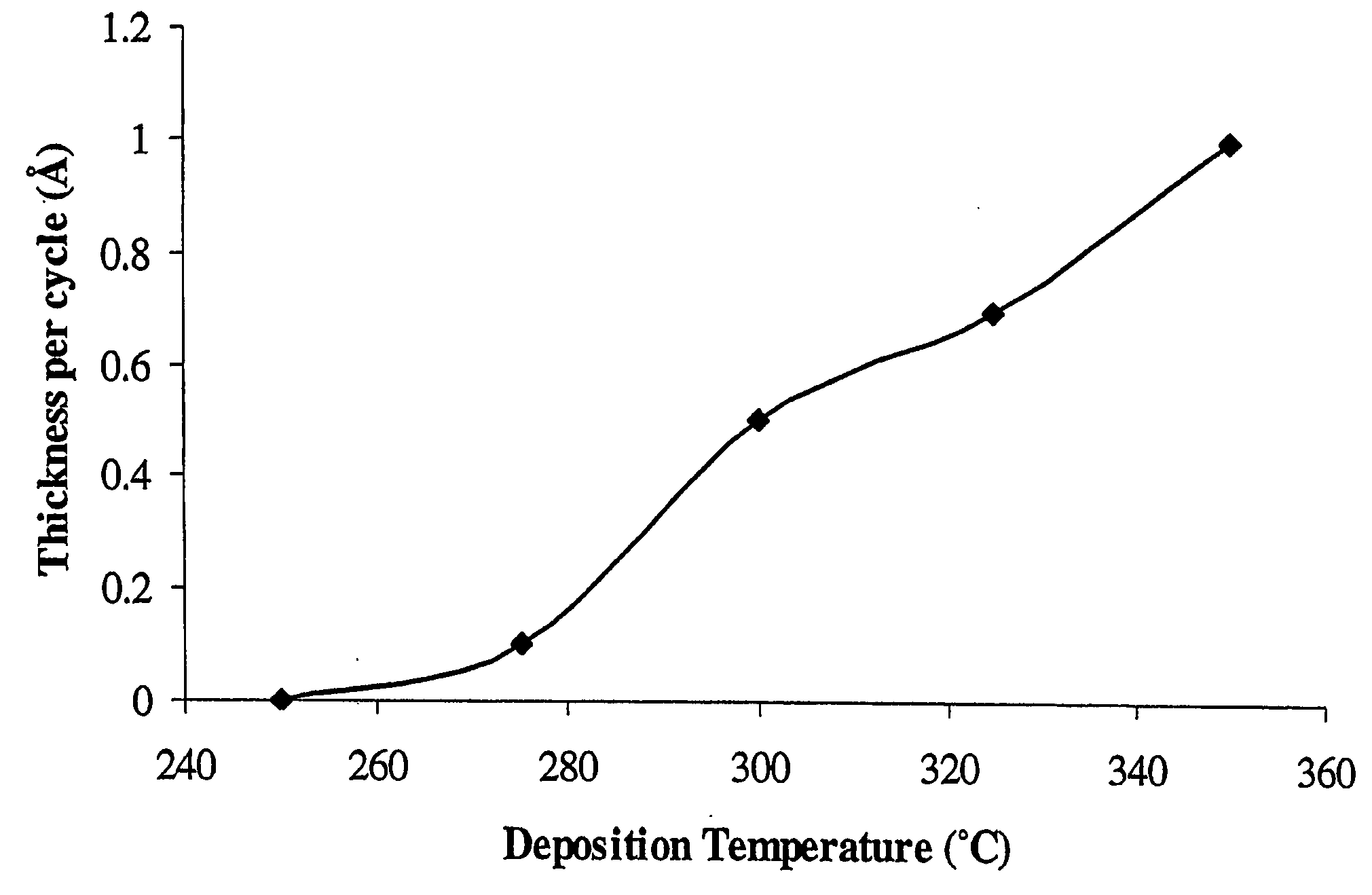
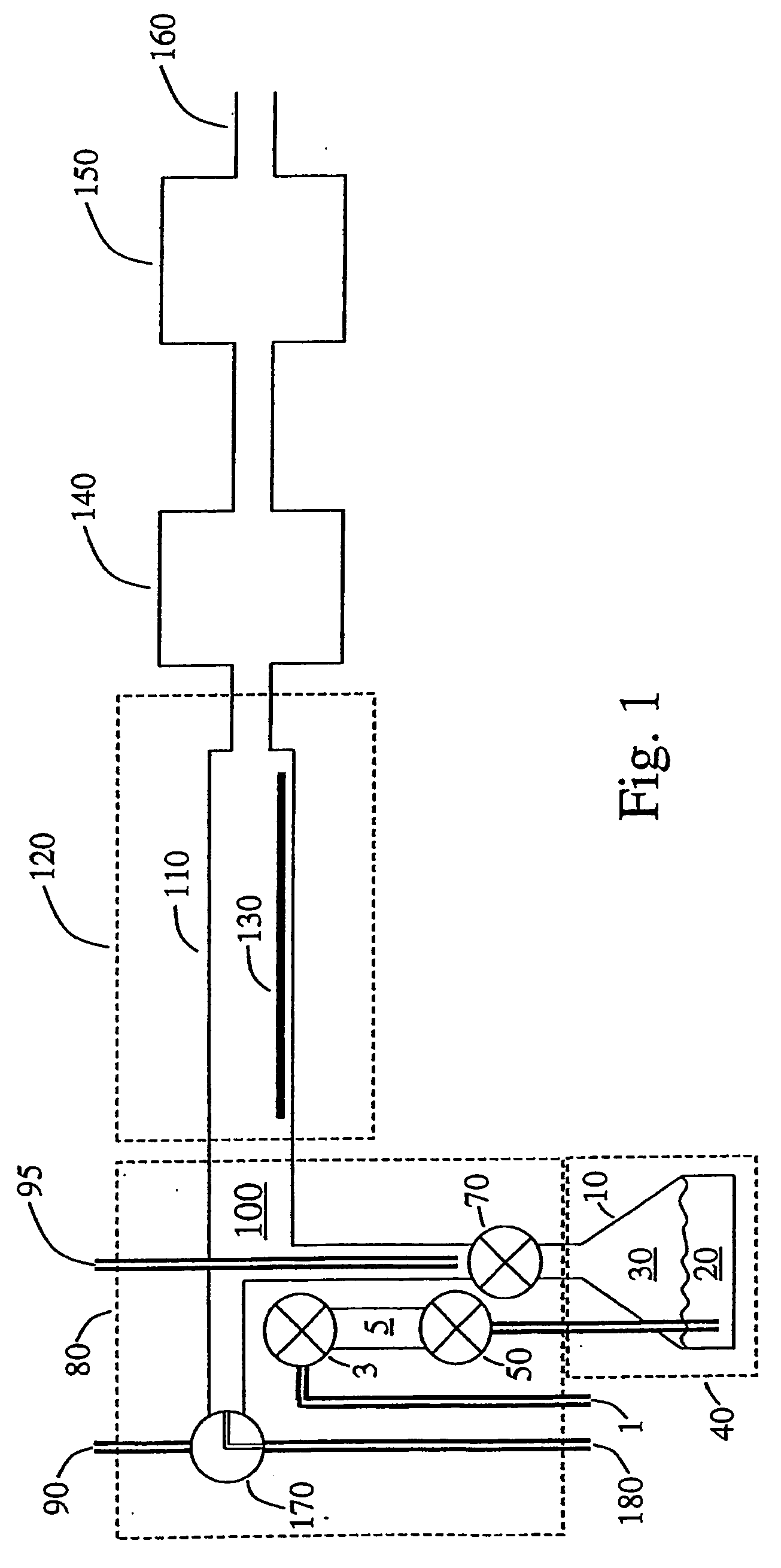
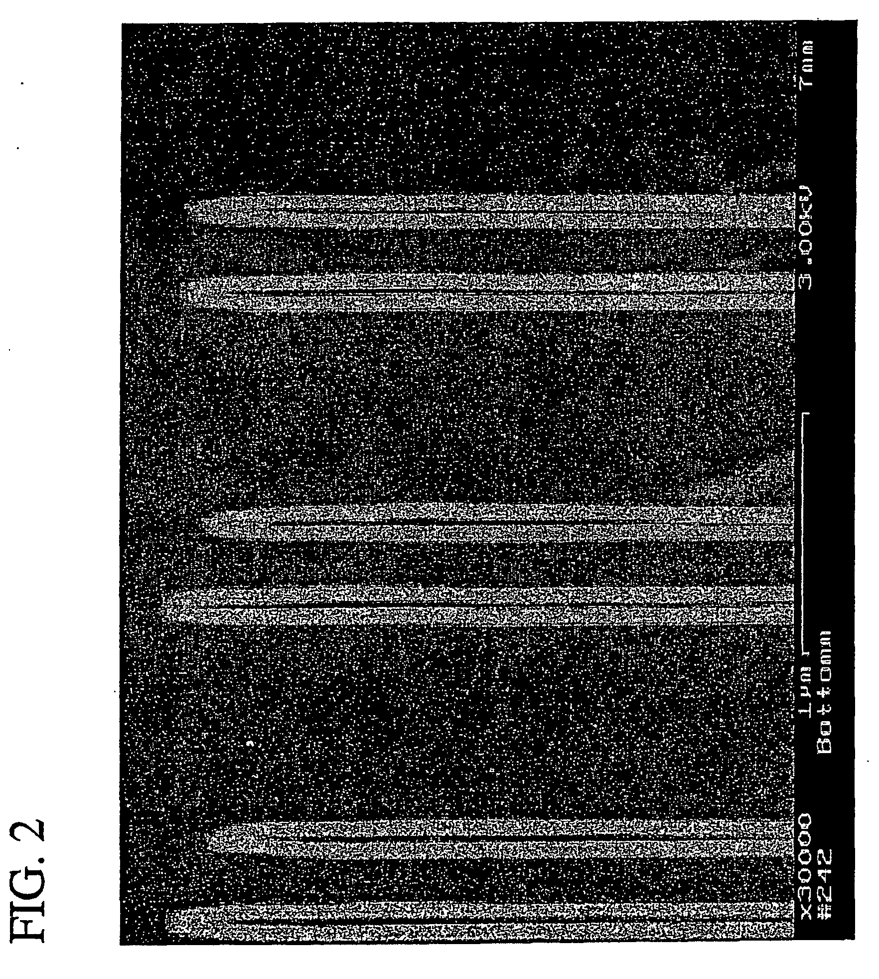
[0049] The apparatus of FIG. 1 was used to deposit tungsten nitride coatings. Bis(tert-butylimido)bis(dimethylamido)tungsten (VI) was placed in a stainless steel container 10 having vapor volume of 0.6 liter and heated to 30° C., at which temperature the tungsten precursor has a vapor pressure of about 6 milliTorr. Ammonia was held in a compressed gas cylinder at 20° C., and passed through a pressure regulator so that its pressure was reduced to 2.4 atmospheres. A silicon substrate 130 was prepared by dissolving its native oxide by placing it in dilute hydrofluoric acid solution for a few seconds. Next the substrate was irradiated by ultraviolet light (e.g. UV mercury lamp) in air until the surface became hydrophilic (about 3 minutes). Then the substrate 130 was placed on a half-round substrate holder 25 cm long in chamber 110 having diameter 2.4 cm and heated over a length 30 cm to a temperature of 300° C. Another silicon substrate with narrow holes (0.1 mic...


PUM

PropertyMeasurementUnit
Temperatureaaaaaaaaaa

Abstract

Tungsten nitride films were deposited on heated substrates by the reaction of vapors of tungsten bis(alkylimide)bis(dialkylamide) and a Lewis base or a hydrogen plasma. For example, vapors of tungsten bis(tert-butylimide)bis(dimethylamide) and ammonia gas supplied in alternate doses to surfaces heated to 300° C. produced coatings of tungsten nitride having very uniform thickness and excellent step coverage in holes with aspect ratios up to at least 40:1. The films are metallic and good electrical conductors. Suitable applications in microelectronics include barriers to the diffusion of copper and electrodes for capacitors. Similar processes deposit molybdenum nitride, which is suitable for layers alternating with silicon in X-ray mirrors.

Description

BACKGROUND OF THE INVENTION [0001] 1. Field of the Invention [0002] This invention relates to materials and processes for deposition of thin films on solid substrates. In particular, this invention relates to materials and processes for deposition of tungsten-containing thin films on solid substrates. This invention also relates to methods and materials for making electrically conducting, conformally deposited films for fabrication of devices in the areas of microelectronics. [0003] 2. Description of the Related Art [0004] Tungsten nitride, WNx, is considered to be a good barrier against diffusion of copper in microelectronic circuits. WNx can also be used in electrodes for thin-film capacitors and field-effect transistors. WNx has been made by reactive sputtering, but the uniformity of film thickness inside narrow features (“step coverage”) is not expected to be adequate for use in future microelectronic devices having narrow features with high aspect ratios. [0005] Atomic layer de...

Claims


Application Information

Patent Timeline
IPC IPC(8): H01L29/40H01L21/44C07F11/00G02B5/08C23C16/34C23C16/44C23C16/455G02B5/26H01L21/02H01L21/28H01L21/285H01L21/768
CPCC07F11/005C23C16/34C23C16/45525C23C16/45534C23C16/45542C23C16/45553H01L21/28088H01L21/28562H01L21/76841H01L28/60H01L29/4966C07F11/00H01L21/02H01L21/768H01L21/0262
Inventor GORDON, ROY G.SUH, SEIGIBECKER, JILL
Owner PRESIDENT & FELLOWS OF HARVARD COLLEGE
Why Eureka
Try Eureka