Air oxidizable scratch resistant protective layer for optical coatings

a protective layer and scratch-resistant technology, applied in the field of outer scratch-resistant protective layers, can solve the problems of frequent damage to optical coatings, high scratching rate of optical coatings, and high scratching rate of metal thin film layers, so as to reduce the damage of scratching damage and ensure the hardness and durability. , the effect of sufficient hardness

Inactive Publication Date: 2006-06-22
AGC FLAT GLASS NORTH AMERICA INC
View PDF34 Cites 74 Cited by
  • Summary
  • Abstract
  • Description
  • Claims
  • Application Information

AI Technical Summary

Benefits of technology

[0015] The primary object of the present invention is to overcome the deficiencies of the prior art described above by providing an air oxidiza

Problems solved by technology

Unfortunately, optical coatings are frequently damaged during shipping and handling by scratching.
Metal thin film layers are well known to be vulnerable to scratch damage.
Thin film stacks consisting of dielectrics or combinations of metal and dielectric layers also frequently suffer from scratching.
This vulnerability to scratching is particularly true of sputtered low-emissivity (also known as “soft” low-e) coatings on architectural glass.
Thus, damage by mechanical abrasion frequently occurs.
Sputtered carbon protect

Method used


Image

  • Air oxidizable scratch resistant protective layer for optical coatings
  • Air oxidizable scratch resistant protective layer for optical coatings
  • Air oxidizable scratch resistant protective layer for optical coatings

Examples


example 1

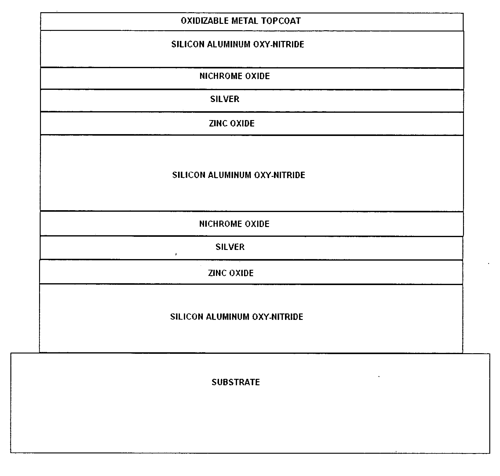
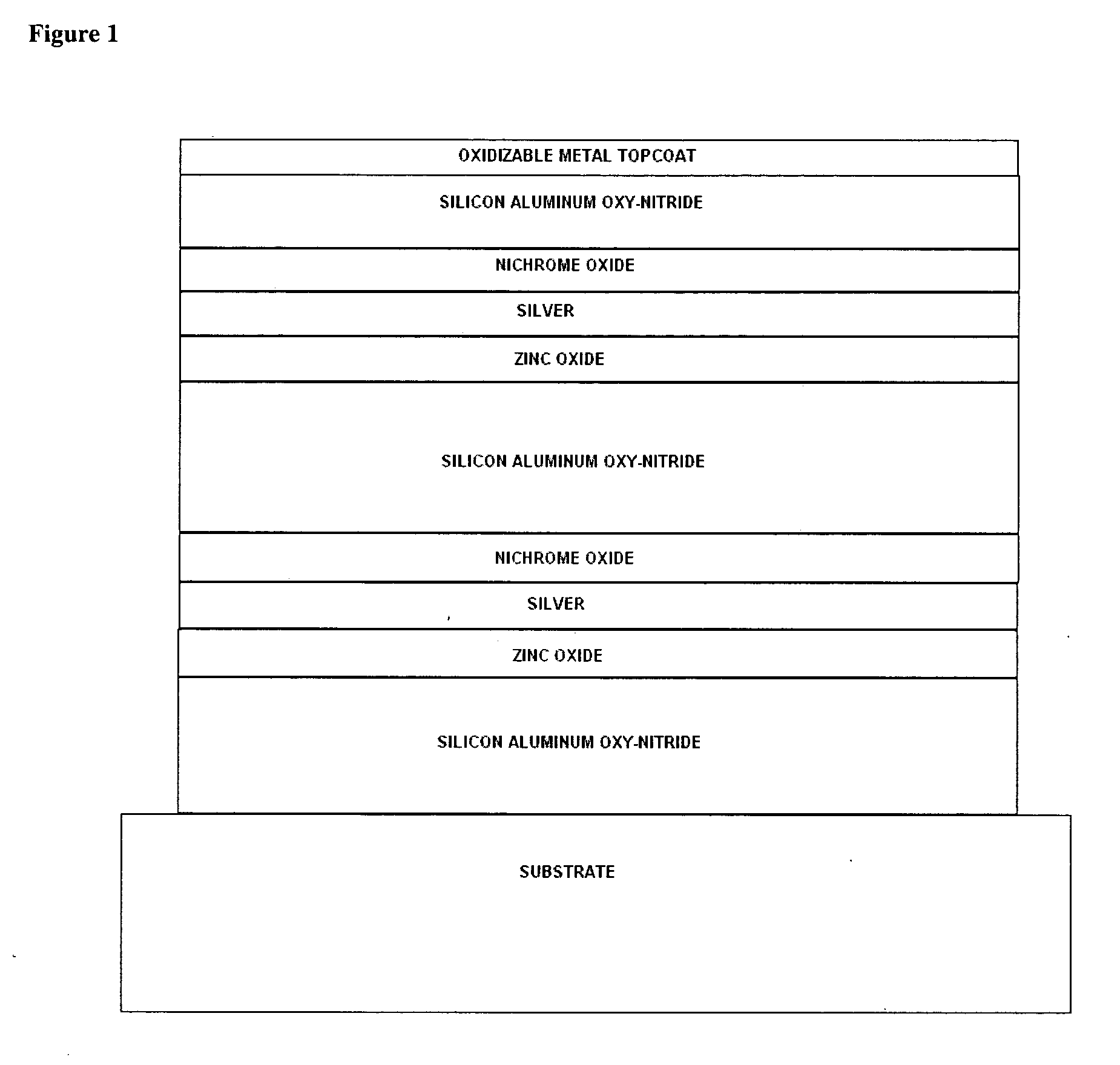
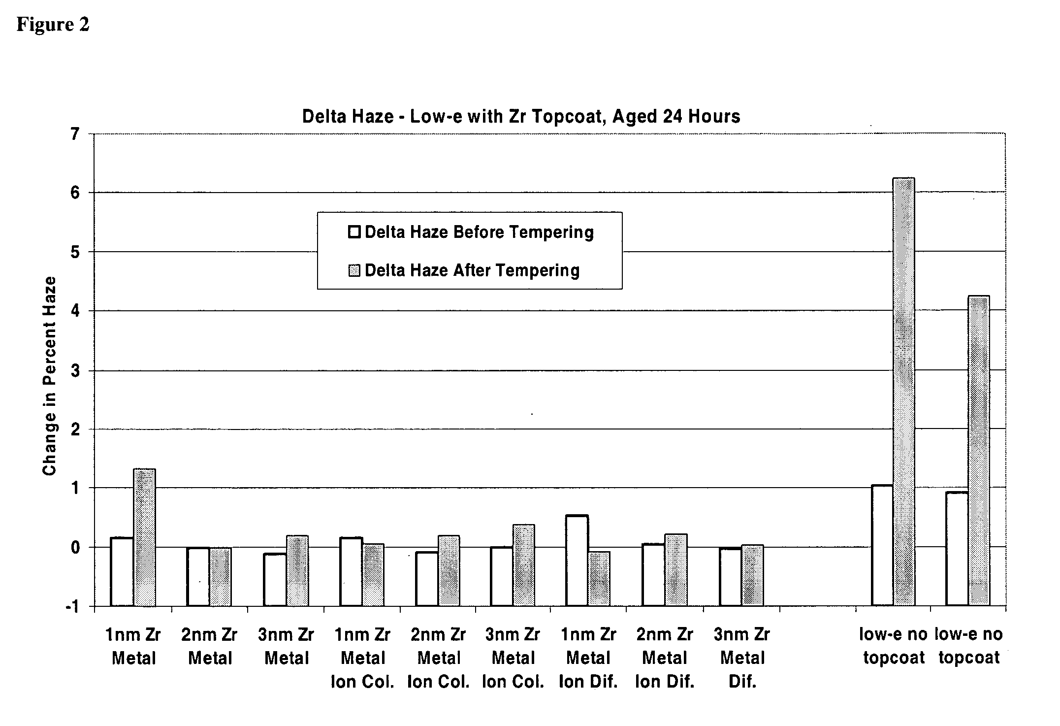
[0071] A low-e structure shown in FIG. 1 is sputtered with an outermost dielectric of silicon nitride. As a last coating step in the vacuum coater, a layer of 2 nm of Zr is deposited on the silicon nitride. The Zr layer oxidizes in air over a period of one week and the transmission of the low-e structure reaches a level within 0.5% of the same non-topcoated low-e.

example 2

[0072] A low-e structure shown in FIG. 1 is sputtered with an outermost dielectric of silicon nitride. As a last coating step in the vacuum coater, a layer of 2.5 nm of Zr is deposited on the silicon nitride. A further oxidation step is carried out in the vacuum coater where the Zr layer is exposed to an oxygen containing plasma. The Zr layer further oxidizes in air over a period of one week and the transmission of the low-e structure reaches a level within 0.5% of the same non-topcoated low-e.

Experimental Procedure:

[0073] Coating setup—Samples were sputter coated using a 1 meter wide Twin-Mag target with Zr targets. Power was AC supplied by a Huttinger BIG 100.

[0074] Samples were sputtered under three different atmospheres: [0075] 1. Argon only to deposit a metal layer. [0076] 2. Addition of small amount (10 sccm) O2 to create oxygen doped Zr. The layer was still substantially metallic. Material is signified in the data as ZrOx. [0077] 3. Addition of small amount (10 sccm) N2 t...

example 3

[0093] Scratch data for low-e stacks with and without topcoats is presented in the table below. The ZrSi topcoat in this case is a co-sputtered layer done on a Twin-Mag where one side of the magnetron is setup with a Zr target and the other side is setup with a Si10wt % Al target. The sputtering of the topcoat is done in an argon atmosphere. Sputtering power was equal on both targets. The resulting topcoats were about 3 nm thick.

[0094] The scratch test was the 200 stroke Scotch-Brite mechanical durability test. In this case the scratch damage on all samples was too low to detect by haze measurements. The quantification was done by a direct count of scratches on the coated surface.

[0095] The counts were carried out by counting all visible scratches across the path of the Scotch-Brite pad path. Counts were taken in three places; one in the center and 1.5 inches to either side of center of the scratched sample. The scratched samples were 4″×6″. The Zr and ZrSi topcoats both provided ...


PUM

PropertyMeasurementUnit
Timeaaaaaaaaaa
Thicknessaaaaaaaaaa
Nanoscale particle sizeaaaaaaaaaa

Abstract

The present invention provides a scratch protecting layer comprising a metal, metal alloy, metal compound or an intermetallic layer deposited on an air contacting surface. The scratch protecting layer is typically from 1 to 3 nanometers thick and not optically absorbing after oxidation occurs. This layer is initially deposited in a primarily unoxidized or un-nitrided state. Full oxidation of the metal, metal alloy, metal compound or intermetallic layer occurs within several days after exposure to air. The scratch protection layer can be 2 to 5 nanometers thick if the layer is exposed to a plasma, electrical discharge or ion beam comprising a reactive gas such as oxygen or nitrogen.

Description

[0001] This application claims the benefit of U.S. Provisional 60 / 636,656 filed Dec. 17, 2004.FIELD OF THE INVENTION [0002] The present invention relates, generally, to outer scratch protective layers which are fully oxidizable without exposure to heat. The outer protective layers are applied on top of optical coatings on various substrates and provide enhanced scratch protection for the layers underneath. In particular, the present invention relates to the use of a metal, metal compound or intermetallic layer as an outer scratch protective layer of an optical coating. DESCRIPTION OF RELATED ART [0003] Low emissivity optical coatings or optical coatings containing infrared reflecting metals, can be deposited on transparent substrates to reduce the transmission of some or all of the infra-red radiation incident on the substrates. Anti-reflected thin silver coatings have been found to reflect a high proportion of infra-red radiation but allow visible light to pass through. These desir...

Claims


Application Information

Patent Timeline
IPC IPC(8): B05D5/06
CPCC03C17/36Y10T428/265C03C17/3626C03C17/3639C03C17/3644C03C17/3652C03C17/366C03C17/3681C03C17/3689C03C2217/78C23C8/02G02B1/105C23C28/321C23C28/322C23C28/34C23C28/345C23C28/3455C03C17/3618G02B1/14C03C17/06C03C17/09B05D5/06B32B17/06
Inventor MASCHWITZ, PETER ALAN
Owner AGC FLAT GLASS NORTH AMERICA INC
Why Eureka
Try Eureka