Method of forming thin film, and method of manufacturing semiconductor device

a technology of semiconductor devices and thin films, which is applied in the direction of semiconductor devices, chemical vapor deposition coatings, coatings, etc., can solve the problems of difficult to apply such a method to mass production, difficult to conduct the impurity removal step using nhsub>3/sub>gas, and conspicuous spoiled output, so as to achieve enhanced yield and suppress leakage current , the effect of enhancing the yield

Inactive Publication Date: 2006-09-07
SONY CORP
View PDF10 Cites 31 Cited by
  • Summary
  • Abstract
  • Description
  • Claims
  • Application Information

AI Technical Summary

Benefits of technology

[0016] As has been described above, according to the method of forming a thin film and the method of manufacturing a semiconductor device of the present invention, the impurity removing treatment can be conducted in the same treatment chamber as that used for the film forming cycle

Problems solved by technology

However, where the annealing treatment is conducted in another chamber by the just-mentioned method, throughput is spoiled conspicuously.
Therefore, it is difficult to apply such

Method used


Image

  • Method of forming thin film, and method of manufacturing semiconductor device
  • Method of forming thin film, and method of manufacturing semiconductor device
  • Method of forming thin film, and method of manufacturing semiconductor device

Examples


first embodiment

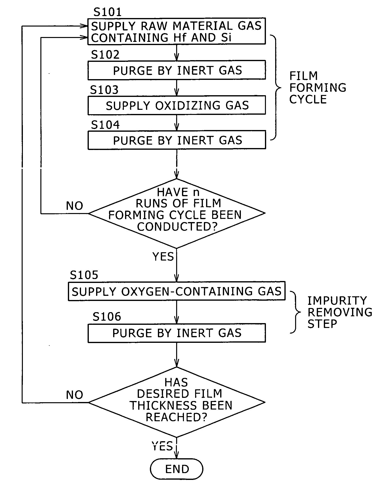
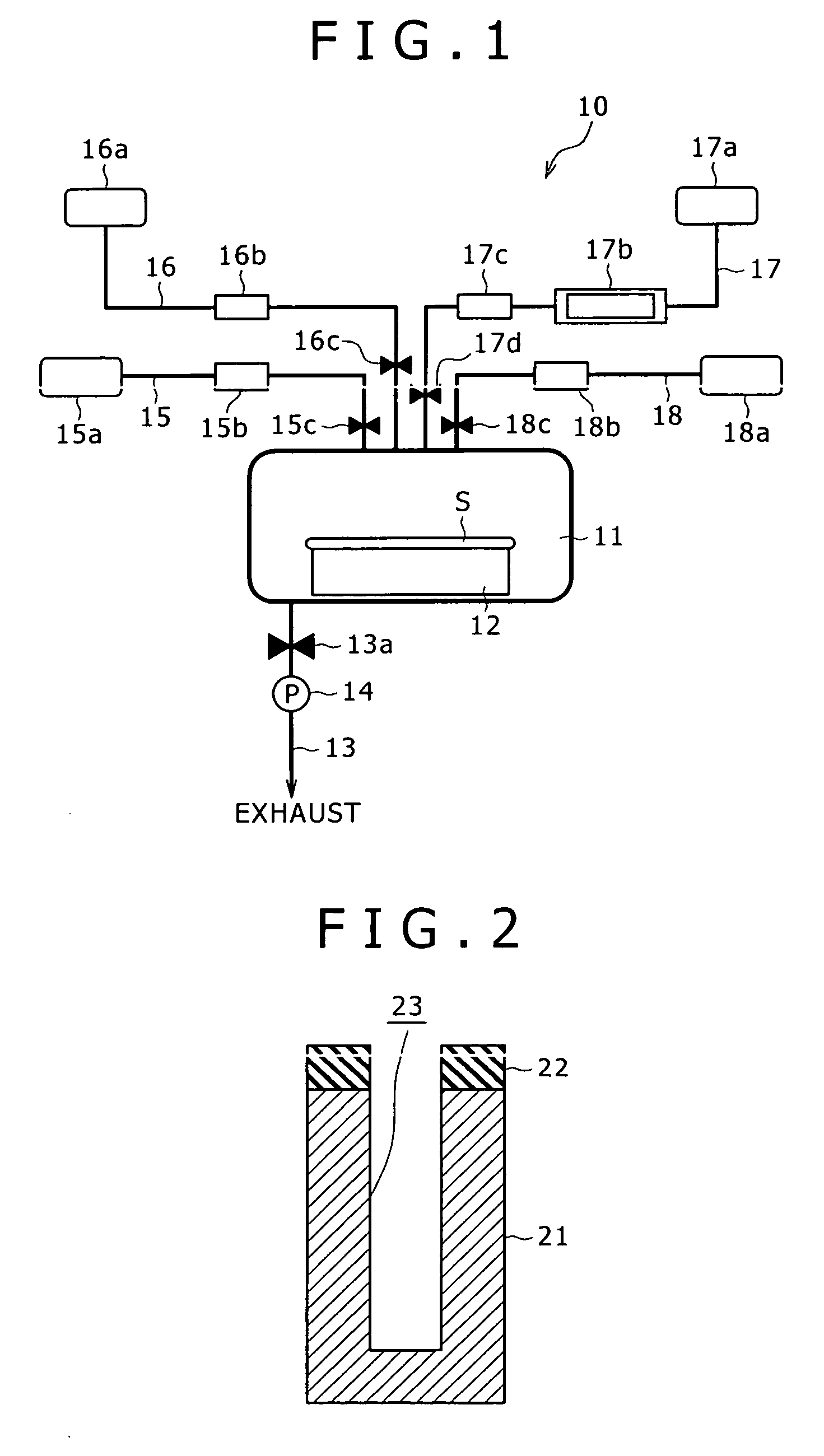
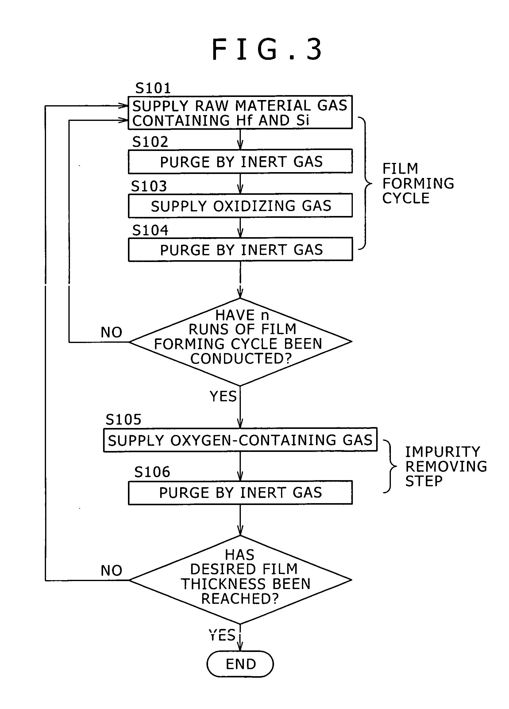
[0030] In this embodiment, in the method of manufacturing a semiconductor device using the first method of forming a thin film according to the present invention, an example of forming a capacitor insulation film of a deep trench type trench capacitor according to an ALD process will be described. As the capacitor insulation film, a film of hafnium silicate (HfSiOx) which is a high-k material is formed. Here, in describing the method of forming the hafnium silicate film by the ALD process, the ALD apparatus used for the film formation will be described referring to the configuration diagram shown in FIG. 1.

[0031] As shown in the figure, the ALD apparatus 10 is a sheet feed type apparatus including a treatment chamber 11 in which to conduct a film forming treatment of a substrate S to be treated. The treatment chamber 11 has a stage 12 on which to mount and hold the substrate S, for example at a bottom portion thereof, and the stage 12 is provided with a heater (omitted in the figur...

second embodiment

[0066] In this embodiment, description will be made of an example in which a gate insulation film of an n-channel MOS field effect transistor (nMOSFET) is formed by an ALD process, in the method of manufacturing a semiconductor device by use of the first method of forming a thin film according to the present invention. As the gate insulation film, a hafnium silicate (HfSiOx) film is formed, in the same manner as in the first embodiment. Here, in forming the hafnium silicate film, the ALD apparatus described referring to FIG. 1 is used.

[0067] First, as shown in FIG. 6A, an SC2 treatment (cleaning with aqueous hydrochloric acid-hydrogen peroxide solution) is applied to the surface of a substrate 31 formed of single crystal silicon, to form an interface layer 32a composed of SiO2. The interface layer 32a is formed to have a film thickness of about 1 nm, independent of the film forming technique, and is further grown through the subsequent film forming treatment and annealing treatment...

third embodiment

[0087] In this embodiment, description will be made of an example in which a capacitor insulation film of a deep trench type trench capacitor is formed by an ALD process, in the method of manufacturing a semiconductor device by use of the second method of forming a thin film according to the present invention. In this embodiment, the same substrate as in the first embodiment (see FIG. 2) is used, and description will be made referring to the flowchart shown in FIG. 7 and the graph of the variation in pressure inside a treatment chamber shown in FIG. 8. Besides, an ALD apparatus used for film formation is configured as shown in FIG. 1.

[0088] First, in the same manner as in the first embodiment, a pretreatment of a substrate 21 is conducted, and thereafter the substrate 21 is mounted and held on a stage 12 in a treatment chamber 11 of an ALD apparatus 10. Then, a capacitor insulation film composed of a hafnium silicate film is formed on a hard mask 22 in the state of covering the ins...


PUM

PropertyMeasurementUnit
Temperatureaaaaaaaaaa
Timeaaaaaaaaaa
Pressureaaaaaaaaaa

Abstract

A method of forming a thin film by use of an ALD process, including: a first step of supplying a raw material gas containing an Hf atom and an Si atom into a treatment atmosphere and adsorbing a raw material gas component onto a surface to be treated of a substrate so as to form a layer containing Hf atoms and Si atoms; a second step of purging by an inert gas; a third step of supplying an oxidizing gas into the treatment atmosphere and permitting the oxidizing gas to react with the raw material gas component adsorbed on the surface to be treated of the substrate so as to form a layer of O atoms; and a fourth step of purging by an inert gas, the film forming cycle of the first to fourth steps being repeated. In the thin film forming method and a semiconductor device manufacturing method, an impurity removing step composed of a fifth step of supplying an oxygen-containing gas into the treatment atmosphere so as to oxidize impurities in the thin film and a sixth step of purging by an inert gas is provided between the fourth step and the first step of the film forming cycle.

Description

CROSS REFERENCES TO RELATED APPLICATIONS [0001] The present invention contains subject matter related to Japanese Patent Application JP 2005-058401 filed in the Japanese Patent Office on Mar. 3, 2005 and Japanese Patent Application JP 2005-366430 filed in the Japanese Patent Office on Dec. 20, 2005, the entire contents of which being incorporated herein by reference. BACKGROUND OF THE INVENTION [0002] The present invention relates to a method of forming a thin film and a method of manufacturing a semiconductor device, particularly to a method of forming a thin film and a method of manufacturing a semiconductor device wherein an insulation film composed of a high-k material is formed by an atomic layer deposition (ALD) process. [0003] Attendant on miniaturization of devices, development of a high-k material as a material for a gate insulation film and a capacitor insulation film has been under way. An insulation film composed of a high-k material is high in dielectric constant; there...

Claims


Application Information

Patent Timeline
IPC IPC(8): H01L21/44
CPCC23C16/401C23C16/45527C23C16/45531H01L21/28194H01L21/3141H01L21/3144H01L21/31612H01L21/31645H01L29/513H01L29/517H01L21/0228
Inventor ANDO, TAKASHIHIRANO, TOMOYUKI
Owner SONY CORP
Why Eureka
Try Eureka