Method of modifying insulating film

a technology of insulating film and treatment step, which is applied in the direction of semiconductor devices, electrical apparatus, transistors, etc., can solve the problems of consuming a large quantity of electric power, generating exponential functional increase of leakage current in direct tunnel, and large problem to be solved, so as to reduce the time of treatment and shorten the treatment time in each modification treatment step.

Active Publication Date: 2006-09-07
TOKYO ELECTRON LTD
View PDF5 Cites 32 Cited by
  • Summary
  • Abstract
  • Description
  • Claims
  • Application Information

AI Technical Summary

Benefits of technology

[0020] According to the present invention, for example, in a method of modifying a gate insulating film of a MOSFET or an interelectrode insulating film of a capacitor used in a memory device, a modification method using a plasma treatment and a modification method using a thermal annealing treatment are combined, whereby the modification effect which has been insufficient only by the modification using a plasma treatment or only by the modification using a thermal annealing treatment can be enhanced.
[0021] According to the present invention, for example, a modification treatment by a plasma treatment and a modification treatment by a thermal annealing treatment are combined, whereby the treatment time in each modification treatment step can be shortened and deterioration in the characteristic of the insulating film, which is caused during a long-time plasma treatment or a long-time thermal annealing treatment, can be suppressed.
[0022] According to the present invention, for example, a step of plasma-treating an insulating film by using a plasma based on a process gas containing a rare gas and oxygen atom for the purpose of removing carbon in the insulating film, and a step of thermally annealing the insulating film in a nitrogen atom-containing gas atmosphere for the purpose of modifying a weak bond such as suboxide or dangling bond in the film to a strong bond by the relaxing effect of heat and suppressing bleed-out of boron from a gate electrode in a P-type MOSFET, can be combined.
[0023] According to the present invention, for example, a step of plasma-treating an insulating film by using a plasma based on a process gas containing nitrogen atom and a rare gas for the purpose of suppressing crystallization of the insulating film caused due to a thermal annealing treatment and suppressing bleed-out of boron from a gate electrode in a P-type MOSFET, and a step of thermally annealing the insulating film in an oxygen atom-containing gas atmosphere for the purpose of modifying a weak bond such as suboxide or dangling bond in the film to a strong bond by the relaxing effect of heat, can be combined.

Problems solved by technology

This is because even a leakage current on a level of causing no actual problem in a conventional device having a relatively low integration degree has a possibility of consuming a large quantity of electric power in a recent miniaturized and / or high-performance device.
Typically, for example, in developing a next-generation MOSFET, thinning of a gate insulating film is approaching the limit with the progress of the above-described miniaturization technique and a large problem to be solved comes out.
That is, as for the process technique, the silicon oxide film (SiO2) used as a gate insulating film at present can be thinned to the extreme (on a level of one- or two-atom layer), but when the film is thinned to a thickness of 2 nm or less, there arises a problem that an exponential functional increase of leakage current is generated by the direct tunnel due to a quantum effect and the power consumption increases.
Typically, when miniaturization of a high-performance silicon LSI is sought for in the process of developing, for example, a next-generation MOSFET, there arises a problem that the leakage current increases and in turn, power consumption increases.
However, in the case where an insulating film using a high-k material expected to ensure such excellent characteristic is formed in practice by a CVD method (chemical vapor deposition) or the like, the film formation is performed at a low temperature so as to enhance the in-plane uniformity and therefore, the obtained film allows for the presence of a large number of non-bonded bonds (dangling bond), weak Si—O bonds (suboxide), carbons contained in the raw material for film formation, or the like and can hardly have good characteristic (Reference Document [1]).
However, the modification treatment by thermal annealing is associated with a problem such as deterioration of the characteristic resulting from crystallization of the insulating film due to a high-temperature process, or increase in the electrical film thickness (lowering of effective dielectric constant) due to oxidation of silicon at the insulating film-silicon interface.
However, the plasma forming method reported at present has a problem such as plasma damage due to high electron temperature or difficulty in large-area formation (Non-Patent Documents 1 and 2).
Also, the electron temperature is low and therefore, the plasma damage brought about as a problem in other plasma forming methods is low.
In practice, studies related to the modification of an insulating film by using this plasma are being made, but a sufficiently high modification effect is not yet attained only by modification using the plasma.

Method used


Image

  • Method of modifying insulating film
  • Method of modifying insulating film
  • Method of modifying insulating film

Examples


examples

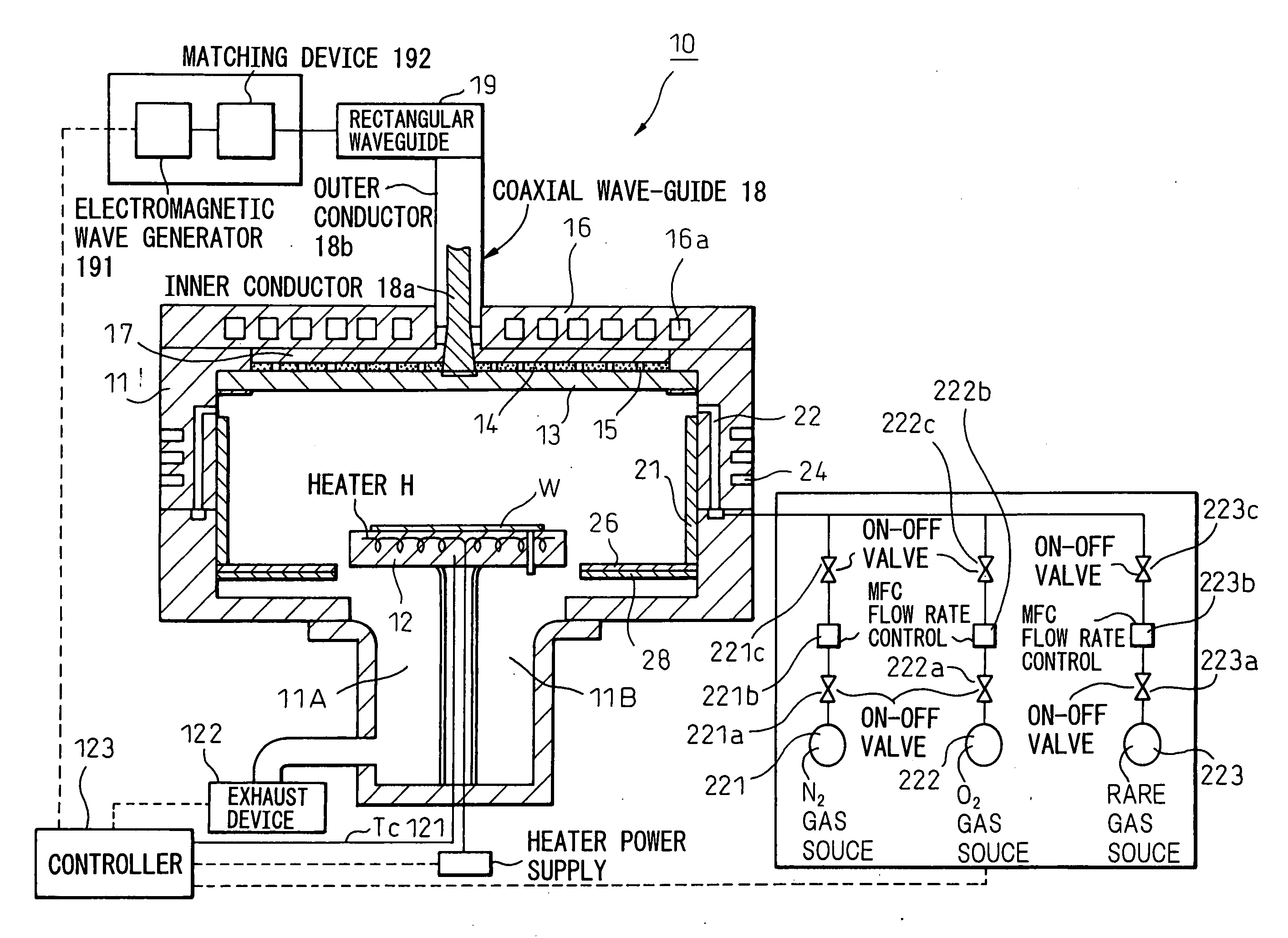
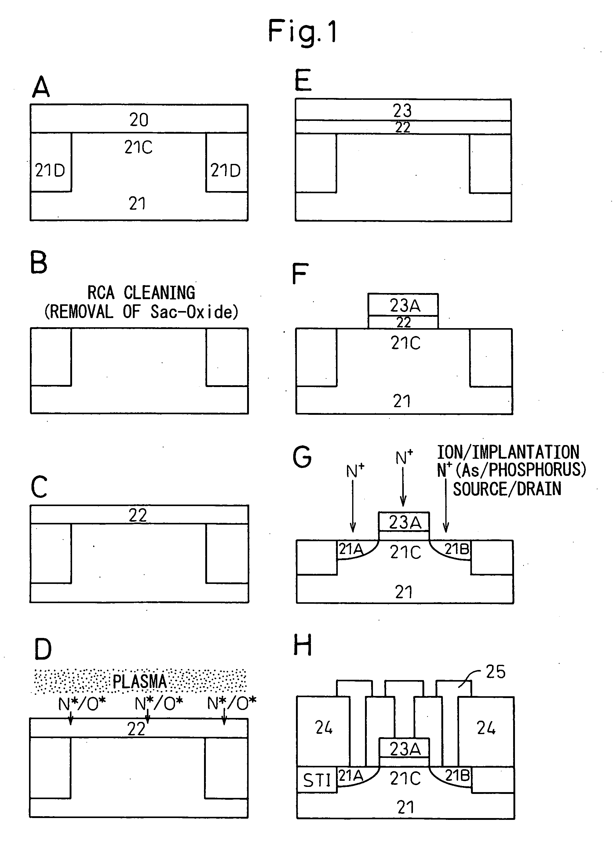
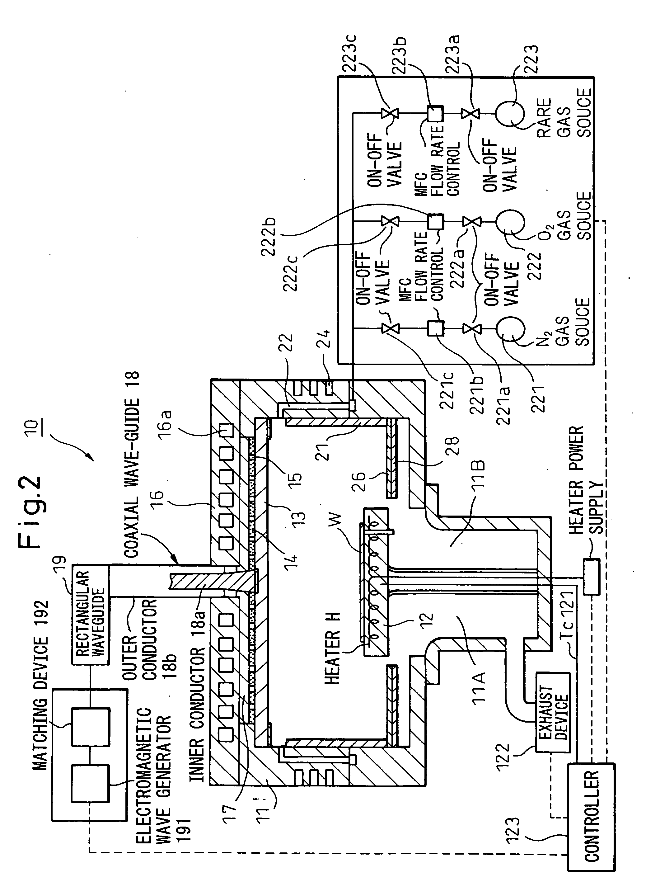
[0090]FIG. 4 shows I-V characteristics of an HfSiO film modified by using the present invention, which is one example of the present invention. In FIG. 4, the ordinate indicates a gate leakage current density of an N-type MOS capacitor comprising a P-type silicon substrate, an HfSiO film and a TiN (titanium nitride) gate electrode, and the abscissa indicates an electric field applied to the insulating film from a polysilicon gate electrode. The production method of the N-type MOS capacitor used in this Example is described below.

[0091] An HfSiO film was formed by a thermal CVD method on a P-type silicon substrate subjected to the same treatments as in FIGS. 1A and 1B. A hafnium tert-butoxide (HTB, Hf(OC4H9)4) and a silane gas (SiH4) were introduced at 1 sccm and 400 sccm, respectively, and the pressure was kept at 50 Pa. The flow rate of HTB is a flow rate on a liquid mass-flow controller and the flow rate of the silane gas is a flow rate on a gas mass-flow controller. In this atmo...


PUM

PropertyMeasurementUnit
temperatureaaaaaaaaaa

Abstract

An insulting film is modified by subjecting the insulting film to a modification treatment comprising a combination of a plasma treatment and a thermal annealing treatment. There is provided a method of enhancing the characteristic of an insulating film by improving deterioration in the characteristic of the insulating film due to carbon, a suboxide, a dangling bond or the like contained in the insulating film.

Description

[0001] This is a continuation-in-part of International Application No. PCT / JP2004 / 007841, filed on May 28, 2004. TECHNICAL FIELD [0002] The present invention relates to a method of modifying an insulating film. More specifically, the present invention relates to a method of enhancing the insulating film modification effect by combining a step of irradiating an insulating film formed by CVD (chemical vapor deposition) or the like with a plasma based on a rare gas-containing process gas, and a step of thermally annealing the insulating film at a high temperature of preferably from 500 to 1,200° C., more preferably from 600 to 1,050° C. The modification method of the present invention can be suitably used particularly when the film obtained by this modification is used for a gate insulating film of a so-called MOSFET (metal-oxide-semiconductor field effect transistor) or for an interelectrode insulating film of a capacitor in a memory device. BACKGROUND ART [0003] The present invention...

Claims


Application Information

Patent Timeline
Patent Type & Authority Applications(United States)
IPC IPC(8): H01L21/00H01L21/28H01L21/314H01L21/316H01L21/8242H01L27/108H01L29/51H01L29/78
CPCH01L21/28176H01L21/28185H01L21/28194H01L21/28202H01L21/28211H01L21/3144H01L21/31658H01L29/518H01L29/78H01L21/02112H01L21/0234
Inventor SUGAWARA, TAKUYATADA, YOSHIHIDENAKAMURA, GENJIOZAKI, SHIGENORINAKANISHI, TOSHIOSASAKI, MASARUMATSUYAMA, SEIJIHASEBE, KAZUHIDENAKAJIMA, SHIGERUFUJIWARA, TOMONORI
Owner TOKYO ELECTRON LTD
Why Eureka
Try Eureka