

Capacitive element, semiconductor device, and method of manufacturing the capacitive element
a capacitive element and semiconductor technology, applied in the direction of capacitors, semiconductor devices, electrical devices, etc., can solve the problem that the performance of the semiconductor device cannot be adequately brought out, and achieve the effect of preventing the peeling of the lower protection insulating film, improving the barrier characteristic and the adhesiveness, and improving the protection insulating film
- Summary
- Abstract
- Description
- Claims
- Application Information
AI Technical Summary
Benefits of technology
Problems solved by technology
Method used
Image

Examples
first embodiment
(2) First Embodiment
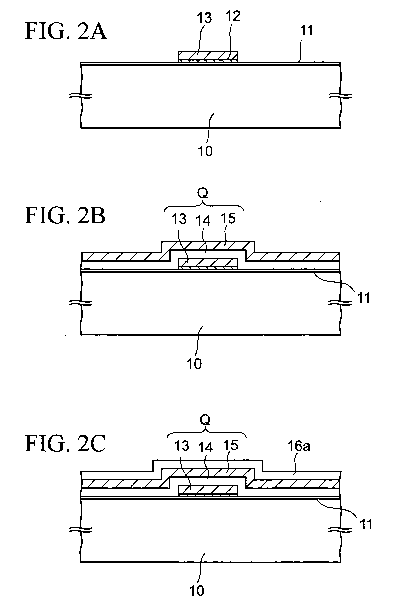
[0036]FIGS. 2A to 2D are sectional views showing a capacitive element according to a first embodiment of the present invention in the course of manufacturing.
[0037] First, steps required until a sectional structure shown in FIG. 2A is obtained will be explained hereunder.
[0038] A thermal oxide film of about 1000 nm thickness is formed by thermally oxidizing a surface of a base member 10 such as a silicon (semiconductor) substrate, or the like, and the thermal oxide film is made into an underlying insulating film 11. Here, as the material constituting the base member 10, a germanium single crystal, a silicon germanium (SiGe), or the like may be employed in place of the silicon single crystal. Also, the base member 10 may be formed of the group III-V compound semiconductor that is made of any one of gallium arsenide (GaAs), indium arsenide (InAs), and indium phosphide (InP).
[0039] In addition, the underlying insulating film 11 is not limited to the thermal oxide...
second embodiment
(3) Second Embodiment
[0065]FIGS. 4A to 4D are sectional views showing a capacitive element according to a second embodiment of the present invention in the manufacturing process.
[0066] This capacitive element is a decoupling capacitor that is packaged on the wiring substrate together with the semiconductor device such as LSI, or the like to absorb the voltage fluctuation, and the like on the power-supply line in LSI.
[0067] At first, steps required until a sectional structure shown in FIG. 4A is obtained will be explained hereunder.
[0068] First, a silicon oxide (SiO2) film of about 500 nm thickness is formed on a base member 20 such as a silicon substrate, or the like by the CVD (Chemical Vapor Deposition) method using a silane as a reaction gas. This film is used as an underlying insulating film 21.
[0069] Then, as a lower electrode 22, a platinum film of about 80 nm thickness is formed on the underlying insulating film 21 by the sputtering method.
[0070] In addition, a high-diel...
third embodiment
(4) Third Embodiment
[0088] The protection insulating film having the double-layered structure explained in the first embodiment can be applied preferably to the semiconductor device such as FeRAM (Ferroelectric Random Access Memory), DRAM (Dynamic Random Access Memory), or the like, in which the capacitor into which the information are written is formed.
[0089] Therefore, in the present embodiment, the case where the protection insulating film having the double-layered structure is applied to FeRAM will be explained hereunder.
[0090]FIGS. 7A to 7L are sectional views showing a semiconductor device according to a third embodiment of the present invention in the manufacturing process. By way of example, explanation will be made hereunder of the stack type FeRAM in which the conductive plug is formed just under the ferroelectric capacitor. But the present invention is not limited to this application, and the present invention can also be applied to the planar type FeRAM.
[0091] First, ...
PUM
 Abstract
Description
Claims
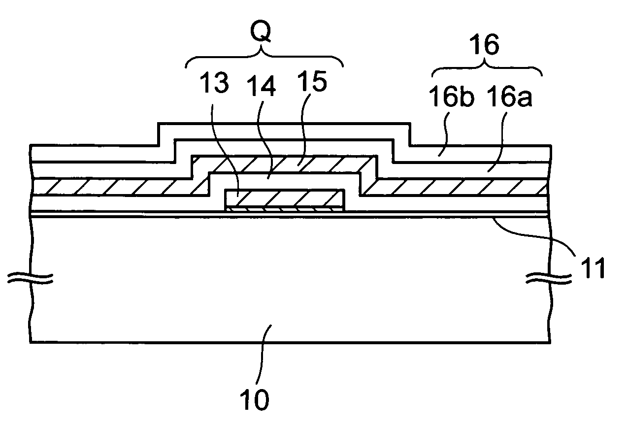
Application Information