

Method for manufacturing carbon fibers and method for manufacturing electron emitting device using the same, method for manufacturing display, and ink for producing catalyst for use in these methods
a technology of carbon fiber and electron emitting device, which is applied in the manufacture of electric discharge tube/lamp, metal/metal-oxide/metal-hydroxide catalysts, etc., can solve the problems of generating corrosive gas to damage the apparatus, difficult to stably form catalyst particles for growing carbon fibers by a solution-applying method, and the lik
- Summary
- Abstract
- Description
- Claims
- Application Information
AI Technical Summary
Benefits of technology
Problems solved by technology
Method used
Image

Examples
example 1
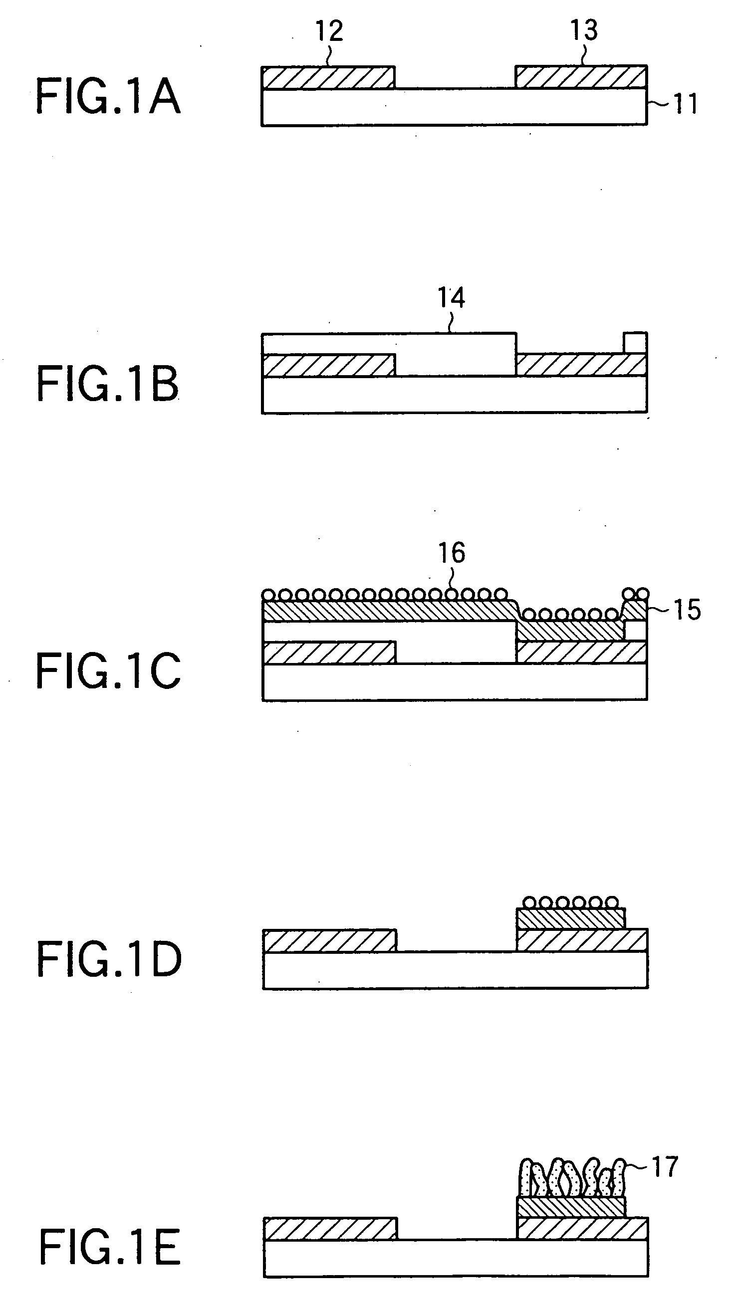
[0100] Following the steps shown in FIGS. 1A to 1E, an electron emitting device was manufactured.
(Step 1)
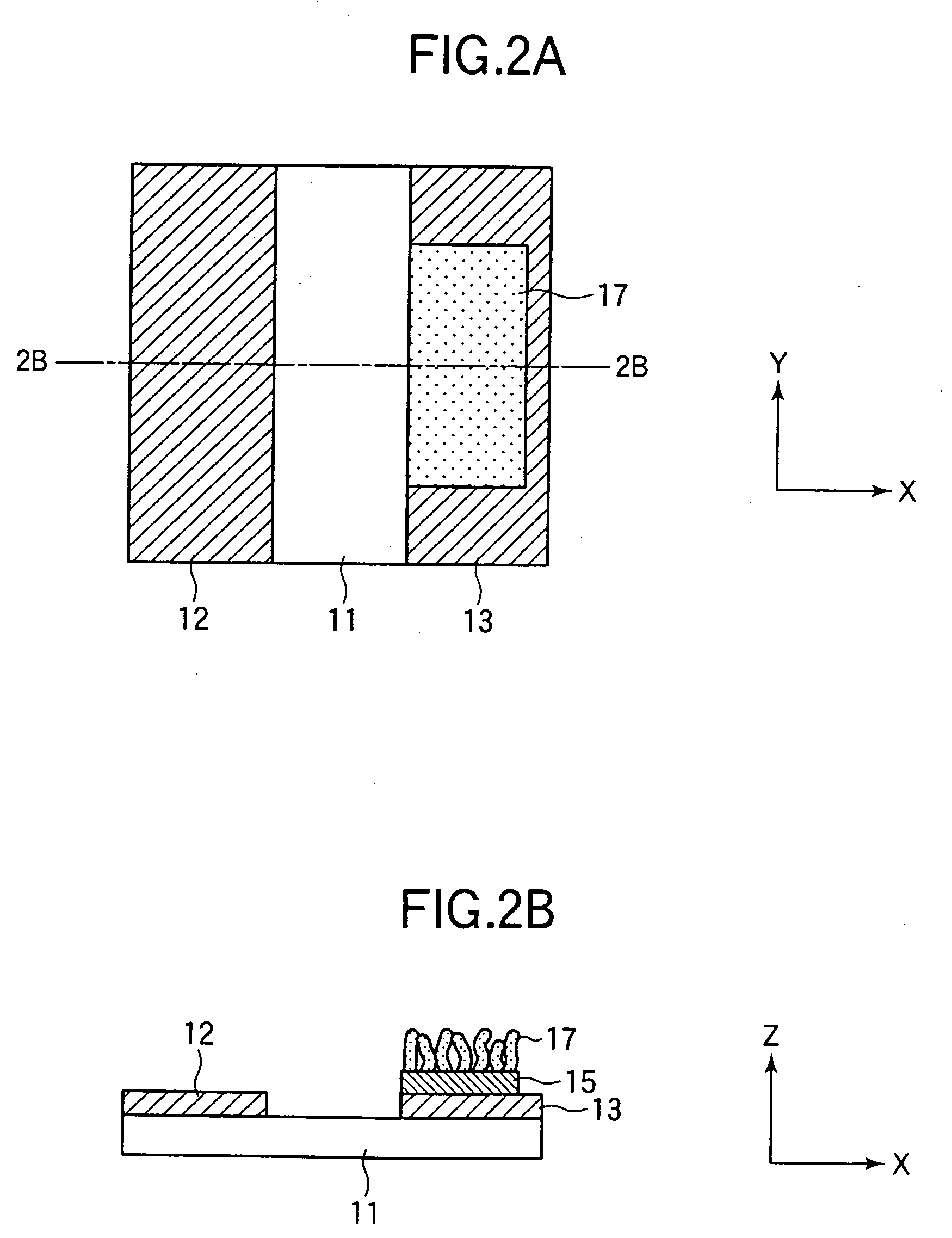
[0101] After an quartz substrate used as the substrate 11 is thoroughly washed, first, an underlying Ti having a thickness of 5 nm and Pt having a thickness of 100 nm not shown in the Figure were continuously vapor-deposited onto all over the substrate by sputtering in order to form the etraction electrode 12 and the cathode electrode 13.
[0102] Next, in a photolithographic step, a resist pattern is formed using a positive photoresist not shown in the Figure.
[0103] Then, using the above patterned photoresist as a mask, the Pt and Ti layers were subjected to a dry etching using Ar gas to pattern the extraction electrode 12 and cathode electrode 13 having a gap between the electrodes (gap width) of 5 μm.
(Step 2)
[0104] In a photolithographic step, a resist pattern 14 is formed using a negative photoresist to be used for subsequent lift-off of an upper layer. Next, a TiN layer...
example 2
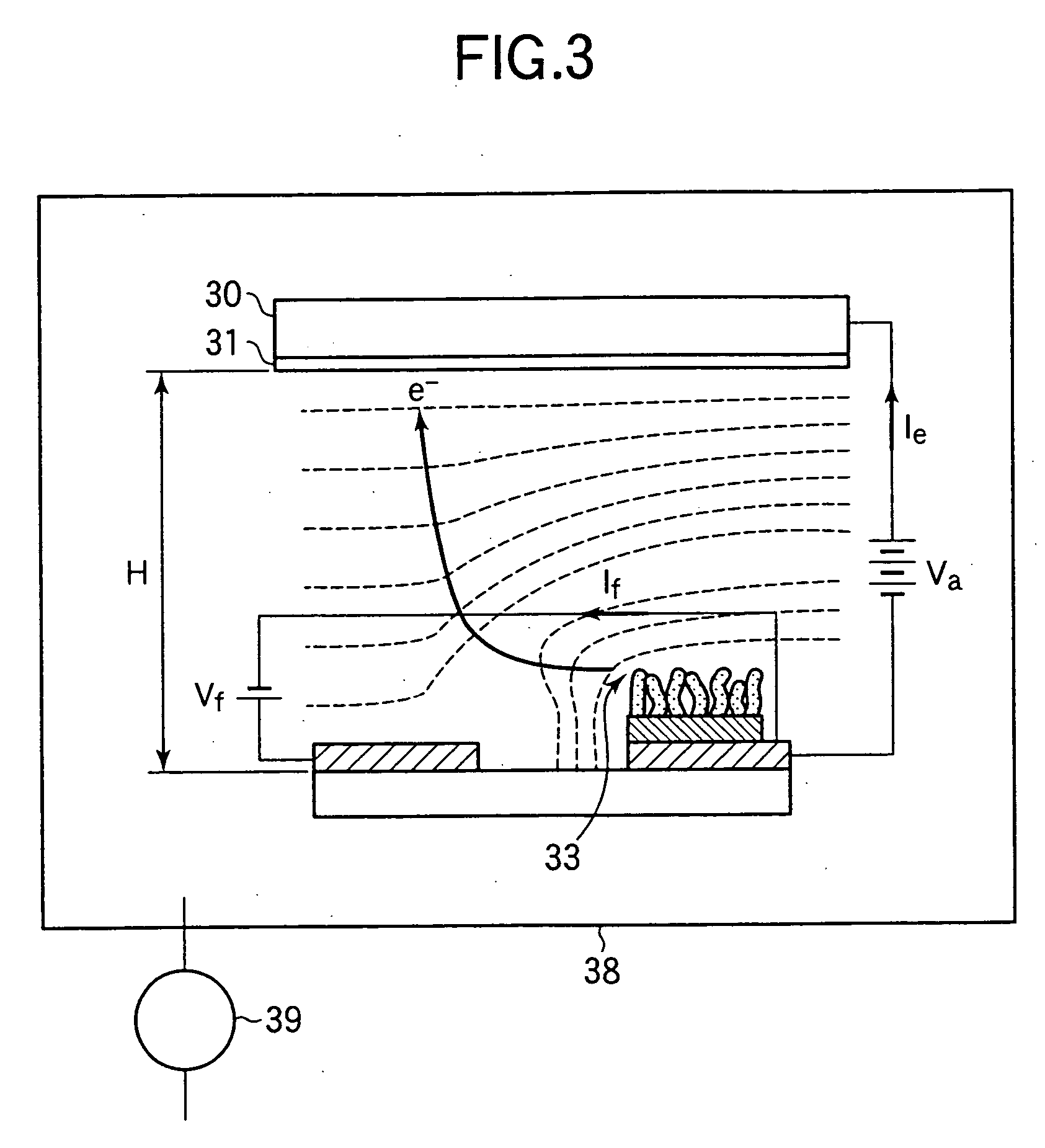
[0110] An electron emitting device was manufactured in the same manner as in Example 1 with the exception that Step 2 was carried out as follows, and If and Ie thereof were measured.
(Step 2)
[0111] In a photolithographic step, a resist pattern 14, is formed using a negative photoresist to be used for subsequent lift-off of an upper layer. Next, a TiN layer was formed as the conductive material layer 15.
[0112] An ink for producing a catalyst was prepared by mixing 0.42 g of cobalt acetate tetrahydrate, 0.05 g of polyvinyl alcohol, 25 g of isopropyl alcohol and 1 g of ethylene glycol and making the whole amount 100 g by addition of water. The ink was spin-coated onto the TiN layer and baked at 350° C. for 30 minutes in the air. According to the above steps, the cobalt oxide particles are produced. Next, the conductive material layer 15 and oxide particles on the resist 14 are lifted off with a peeling liquid for the resist, and then a heating process is carried out at 600° C. in a ...
example 3
[0115] An electron emitting device was manufactured in the same manner as in Example 1 with the exception that Step 2 was carried out as follows, and If and Ie thereof were measured.
(Step 2)
[0116] In a photolithographic step, a resist pattern 14 is formed using a negative photoresist to be used for subsequent lift-off of an upper layer. Next, a TiN layer was formed as the conductive material layer 15.
[0117] An ink for producing a catalyst was prepared by mixing 0.42 g of nickel acetate tetrahydrate, 0.05 g of polyacrylic acid, 25 g of isopropyl alcohol and 1 g of ethylene glycol and making the whole amount 100 g by addition of water. The ink was spin-coated onto the TiN layer and baked at 350° C. for 30 minutes in the air, and then the resulting ink was subjected to a reduction treatment at 600° C. in a hydrogen stream to form catalyst particles. When the particles were observed on a scanning electron microscope (SEM), Ni particles were formed on the TiN layer.
[0118] If and Ie ...
PUM
| Property | Measurement | Unit |
|---|---|---|
| electric field | aaaaa | aaaaa |
| thickness | aaaaa | aaaaa |
| gap width | aaaaa | aaaaa |
Abstract
Description
Claims
Application Information