Photomask blank, photomask and fabrication method thereof

a technology of photomask and resist film, which is applied in the direction of photomechanical equipment, originals for photomechanical treatment, instruments, etc., can solve the problems of reducing the precision of the transfer of photomask pattern onto the resist film, affecting the effect of etching rate, and affecting the quality of photomasks. , to achieve the effect of reducing the damage occurring during etching, reducing the amount of metal, and high etching ra

Active Publication Date: 2007-01-25
SHIN ETSU CHEM IND CO LTD +1
View PDF4 Cites 54 Cited by
  • Summary
  • Abstract
  • Description
  • Claims
  • Application Information

AI Technical Summary

Benefits of technology

[0040] The phase-shift mask blank according to the present invention has a light-shielding film having a thickness of 60 nm or less that has a high etching rate and a low metal percentage content and is formed on the translucent film containing both silicon and molybdenum. Thus, if a thin photoresist film (for example, a chemically amplified photoresist film having a thickness of 250 nm or less) is formed by application and used as a mask, the damage occurring during etching is substantially reduced.
[0041] As described above, the phase-shift mask blank according to the present invention achieves an increased dry-etching rate by adapting the thickness and composition of each layer to provide a desired optical characteristic and by providing a light-shielding film having a low metal percentage content. Therefore, the load on the photoresist, which is used as a mask for forming a photomask pattern, during dry etching is reduced, a practically acceptable level of etching resistance is assured, and thus, the thickness of the photoresist film can be reduced. That is, according to the present invention, reduction in thickness of the photoresist film, which is required for forming a fine photomask pattern with high precision, is achieved.
[0042] According to the present invention, the dry-etching rate is increased by reducing the chromium content (increasing the lig

Problems solved by technology

Thus, if reduction projection exposure is performed using a photomask that has a photomask pattern formed from a circuit pattern on a semiconductor substrate through 4-fold magnification is used to perform, the photomask pattern cannot be faithfully transferred onto the resist film due to interference of the exposure light or the like.
In general, as the aspect ratio of the resist pattern increases, the pattern becomes more susceptible to degradation, and if the resist pattern is used as the etching mask, the precision of the transfer thereof onto the light-shielding film decreases.
In an extreme case, a part of the resist pattern may fall or peel off, resulting in a defective pattern.
However, such etching often has a significant effect on an organic film, such as the photoresist.
Thus, if the light-shielding film made of a chromium compound is etched using a relatively thin resist film as a mask, the resist is damaged during the etching, the configuration of the resist pattern changes, and it is difficult to accurately transfer the original resist pattern onto the light-shielding film.
However, it is technically difficult to make the photoresist, which is an organic film, have both high resolution and patterning precision and high etching resistance.
As far as a conventional patterning process is used, there exists a

Method used


Image

  • Photomask blank, photomask and fabrication method thereof
  • Photomask blank, photomask and fabrication method thereof
  • Photomask blank, photomask and fabrication method thereof

Examples


example 1

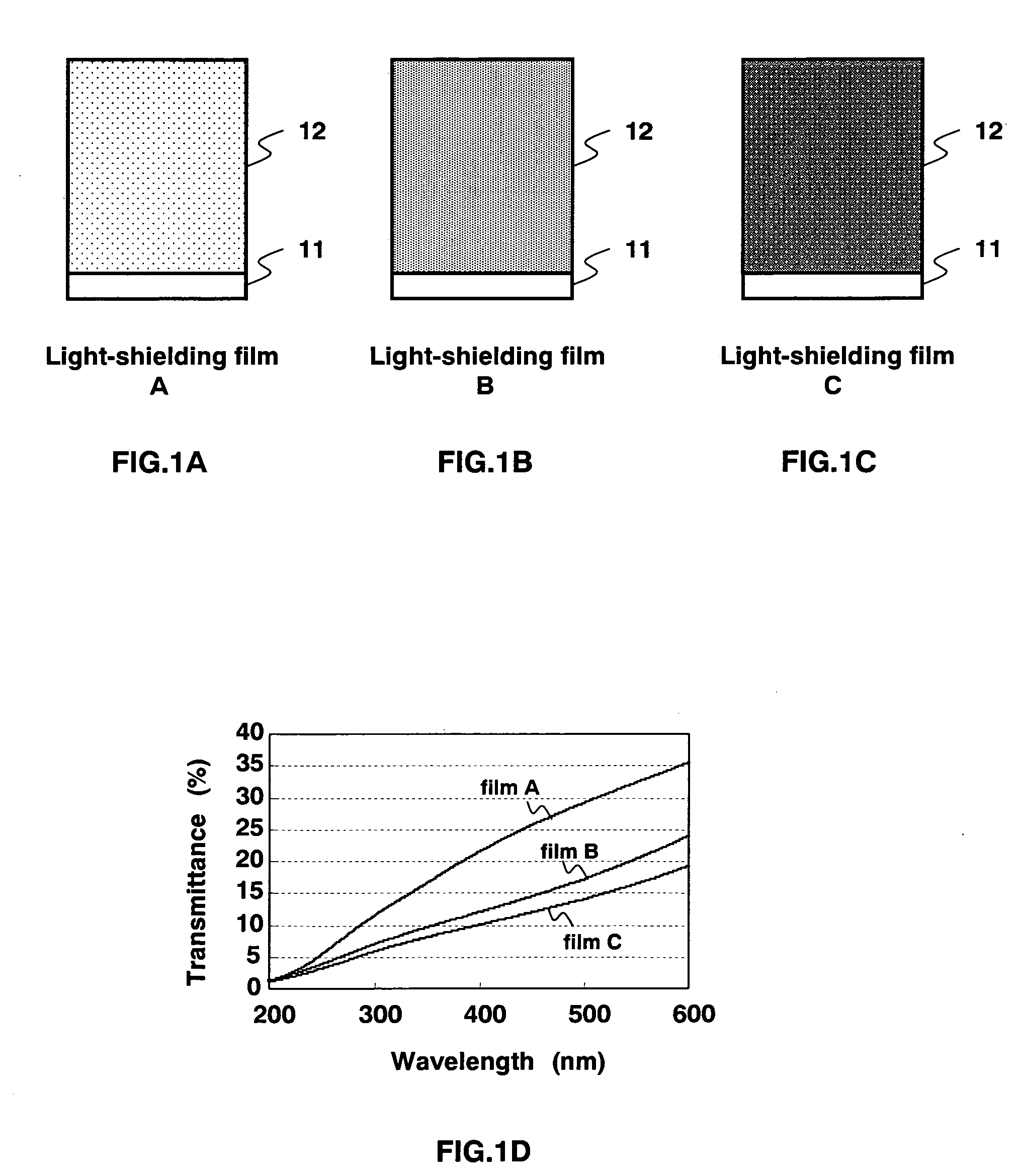
Light-shielding Film of Photomask Blank According to Present Invention

[0067] In order to enable reduction of the thickness of a photoresist used as a mask for forming a photomask pattern, damage to the photo resist during etching of the light-shielding film that is patterned using the photoresist mask has to be reduced. To this end, it is essential to reduce the time required for etching of the light-shielding film by reducing the physical thickness of the light-shielding film to be patterned and / or by increasing the etching rate of the light-shielding film.

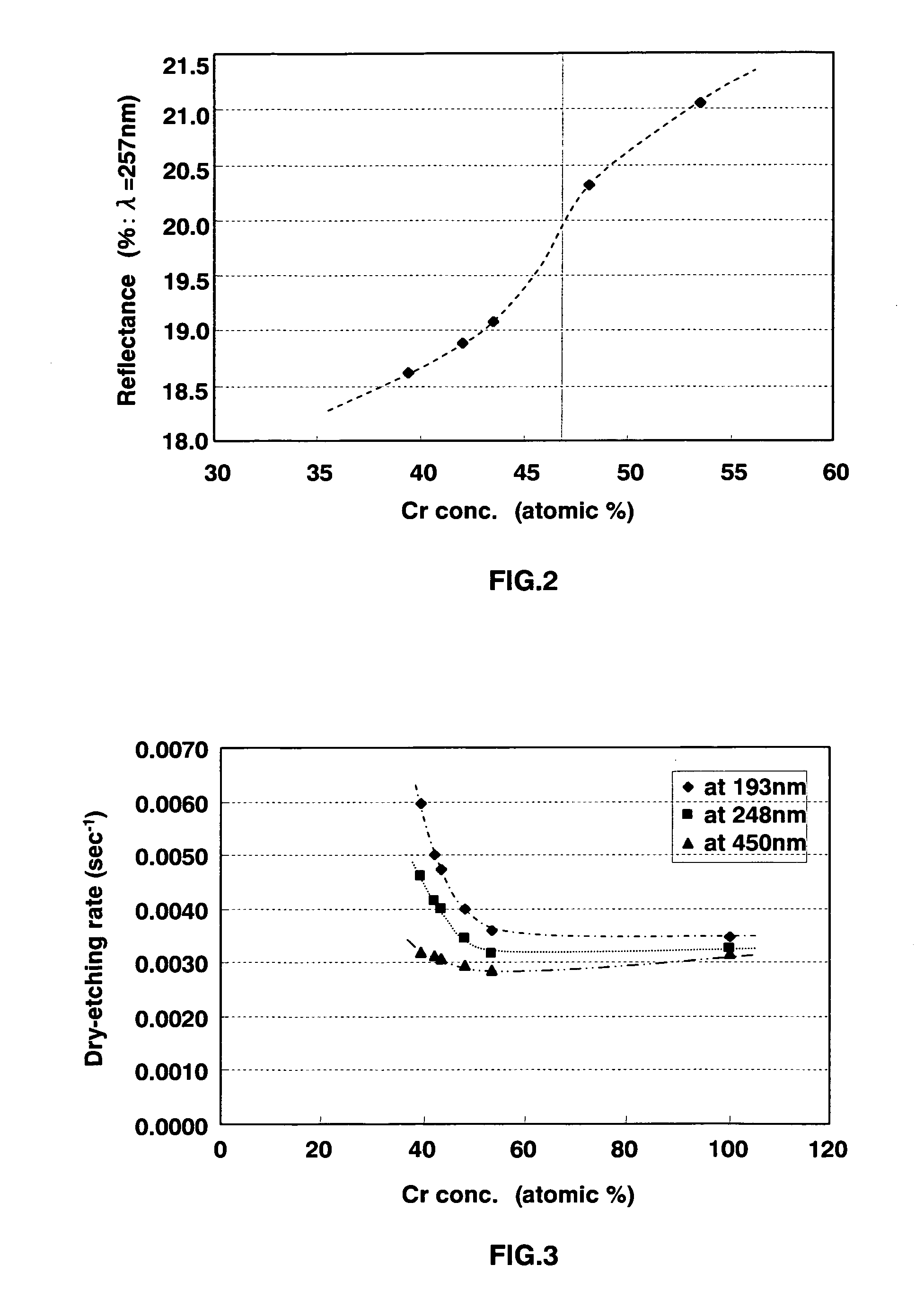
[0068] Investigations by the inventors have proven that the etching rate of the light-shielding film can be achieved by reducing the metal percentage content of the film. This means that high-rate etching can be achieved by designing a chromium-based light-shielding film, which is commonly used, to reduce the chromium content (percentage content) of the film.

[0069] For example, in the case where a light-shielding film of a ch...

example 2

Basic Structure of Photomask Blank

[0120]FIG. 9A is a schematic cross-sectional view for illustrating an exemplary structure of a photomask blank according to the present invention, in which a light-shielding film 12 is formed on one principal plane of a transparent substrate 11 made of quartz or the like that serves as a photomask substrate. The light-shielding film 12 has the layered structure described above with regard to the example 1 and can serve not only as a “light-shielding film” but also as an antireflection film. The film of such a composition is used because it has excellent characteristics including dry etching characteristics, conductivity, and chemical resistance.

[0121] In the case where the photomask blank according to the present invention is designed for fabrication of a mask for ArF exposure, the thickness and composition of the light-shielding film 12 are selected so that the optical density OD of the light-shielding film 12 for light having a wavelength of 19...

example 3

Photomask Blank, and First Example of Patterning Process

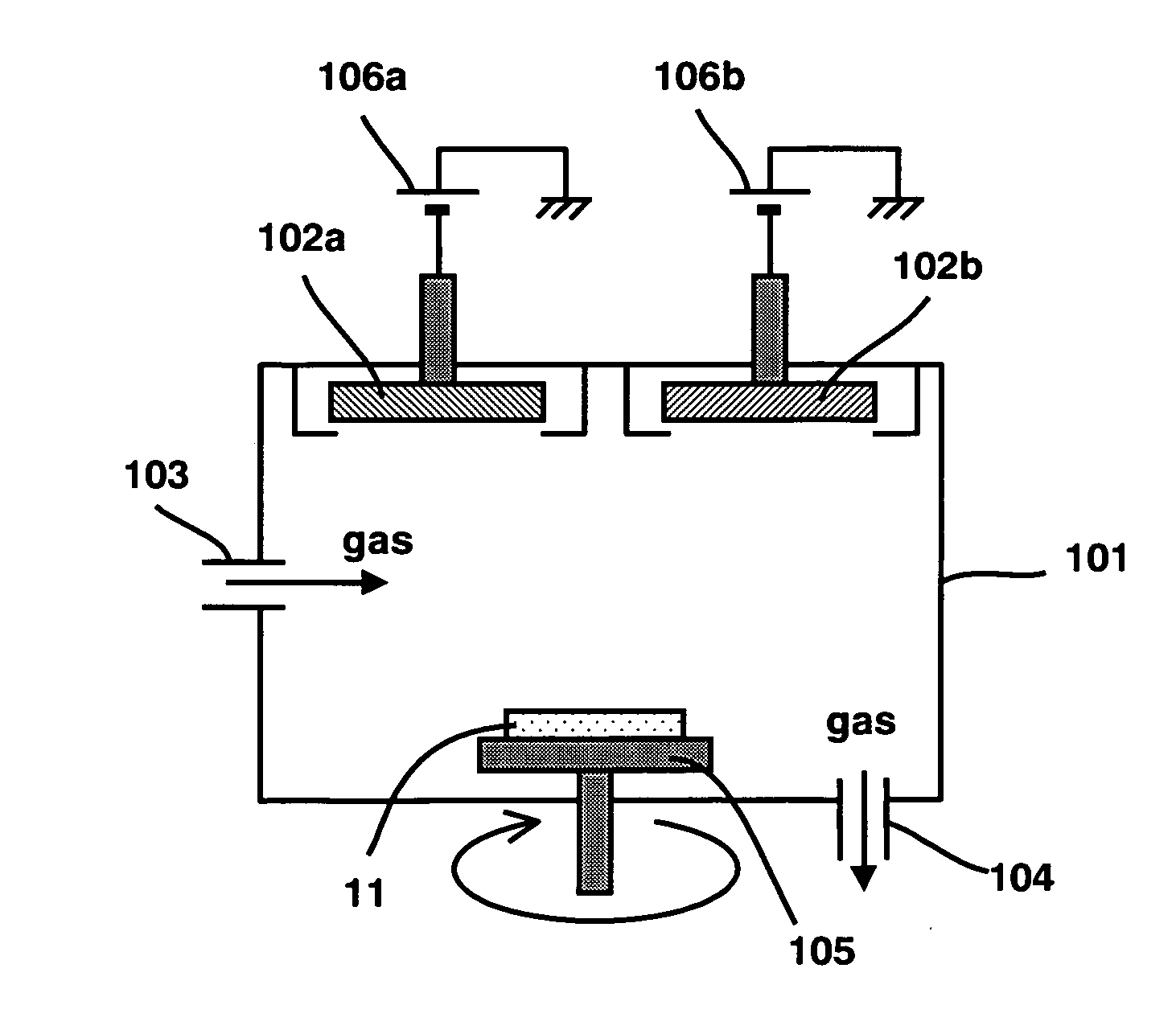
[0131]FIG. 10 shows an exemplary arrangement of a film deposition apparatus (sputtering apparatus) used for fabricating a photomask blank according to the present invention, and FIGS. 11A to 11D are diagrams for illustrating an exemplary process of patterning the photomask blank.

[0132] In FIG. 10, reference numeral 11 denotes a transparent substrate, which is a 6-inch rectangular quartz substrate. Typically, the surface and end faces of the quartz substrate are finely polished. Reference numeral 101 denotes a chamber, reference numeral 102a denotes a first target, reference numeral 102b denotes a second target, reference numeral 103 denotes a sputtering gas inlet, reference numeral 104 denotes a gas outlet, reference numeral 105 denotes a substrate turntable, and reference numerals 106a and 106b denote power supplies that apply a bias to the first and second targets, respectively.

[0133] The first target 102a and the second ...


PUM

PropertyMeasurementUnit
Fractionaaaaaaaaaa
Thicknessaaaaaaaaaa
Thicknessaaaaaaaaaa

Abstract

A light-shielding film for exposure light is formed on one principal plane of a transparent substrate made of quartz or the like that serves as a photomask substrate. The light-shielding film can serve not only as the so-called “light-shielding film” but also as an anti-reflection film. In addition, the light-shielding film has a total thickness of 100 nm or less, 70% or more of which is accounted for by the thickness of a chromium compound that has an optical density (OD) per unit thickness of 0.025 nm−1 for light having a wavelength of 450 nm. In the case where the photomask blank is used for fabricating a mask designed for ArF exposure, the thickness and composition of the light-shielding film are selected in such a manner that the OD of the light-shielding film is 1.2 to 2.3 for 193 or 248 nm wavelength light.

Description

BACKGROUND OF THE INVENTION [0001] 1. Field of the Invention [0002] The present invention relates to a photomask, a photomask blank, which is a raw material of the photomask, and fabrication methods thereof. [0003] 2. Description of the Related Art [0004] In recent years, in order to meet the demand for miniaturization of circuit patterns required for increasing the packaging density of large-scale integrated circuits, advanced semiconductor micromachining techniques have become extremely important. For example, increasing the packaging density of a large-scale integrated circuit essentially requires a technique of thinning wires of wiring patterns in the circuit or a technique of miniaturizing a contact hole pattern for interlevel wiring of a cell. The trend toward miniaturization of circuit patterns of large-scale integrated circuits is being accelerated because it is the most effective approach to increase the operation speed thereof and reduce the power consumption thereof. [000...

Claims


Application Information

Patent Timeline
IPC IPC(8): B32B9/00B32B17/10B32B17/06G03F1/00
CPCG03F1/32Y10T428/24917G03F1/54G03F1/46G03F1/58Y10T428/31616G03F1/26G03F1/38
Inventor YOSHIKAWA, HIROKIKUBOTA, HIROSHIKINASE, YOSHINORIOKAZAKI, SATOSHIMARUYAMA, TAMOTSUHARAGUCHI, TAKASHIIWAKATA, MASAHIDEFUKUSHIMA, YUICHISAGA, TADASHI
Owner SHIN ETSU CHEM IND CO LTD
Why Eureka
Try Eureka