

Method and apparatus for evaluating semiconductor layers
a semiconductor layer and method technology, applied in the direction of color/spectral properties measurement, material analysis, instruments, etc., can solve the problems of degrading the pulse response characteristics of hemt devices, affecting the processing efficiency of hemt devices, etc., to achieve simple constitution, easy introduction to mass production lines, and high data acquisition throughput
- Summary
- Abstract
- Description
- Claims
- Application Information
AI Technical Summary
Benefits of technology
Problems solved by technology
Method used
Image

Examples
embodiment 1
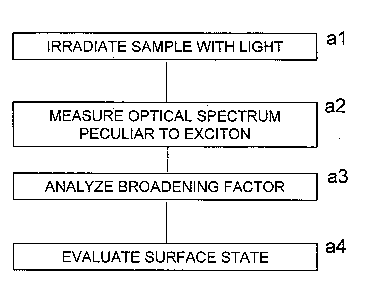
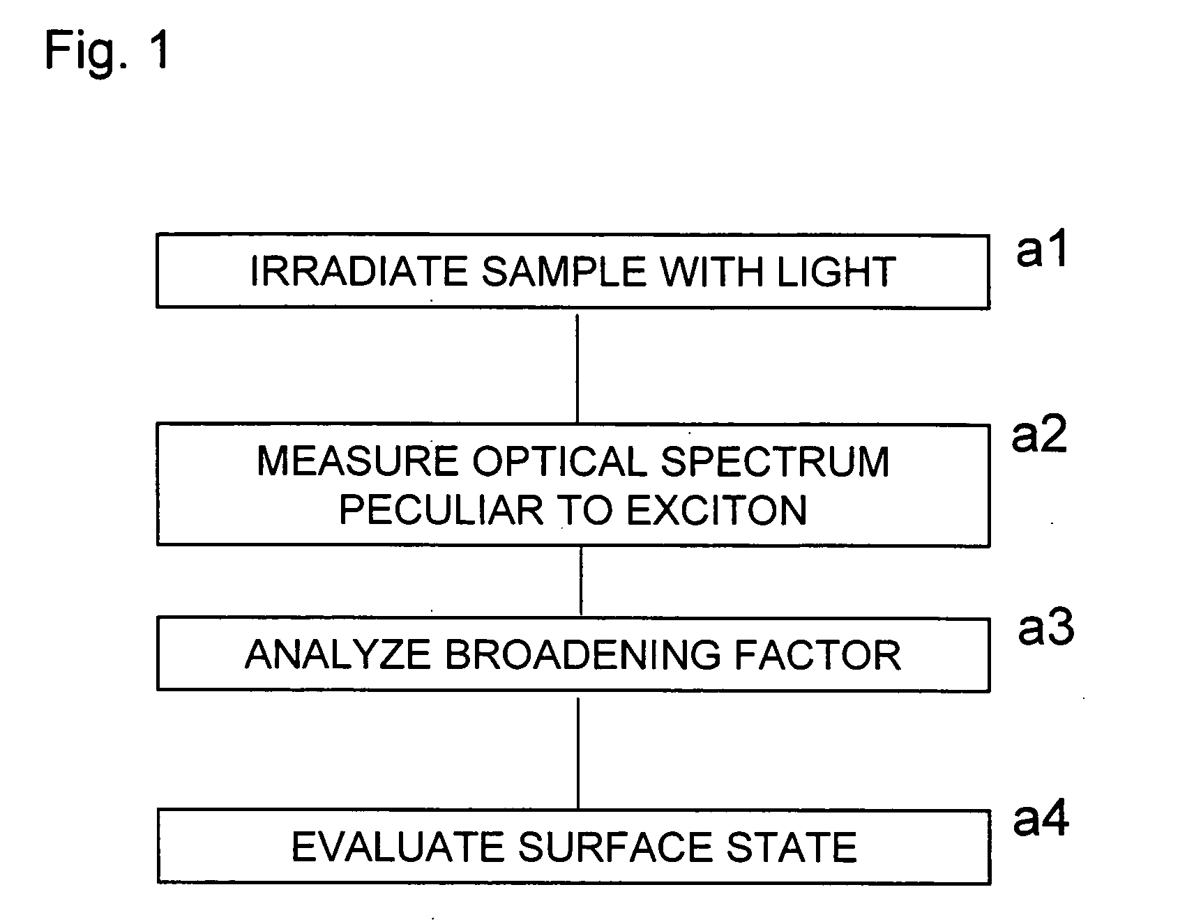
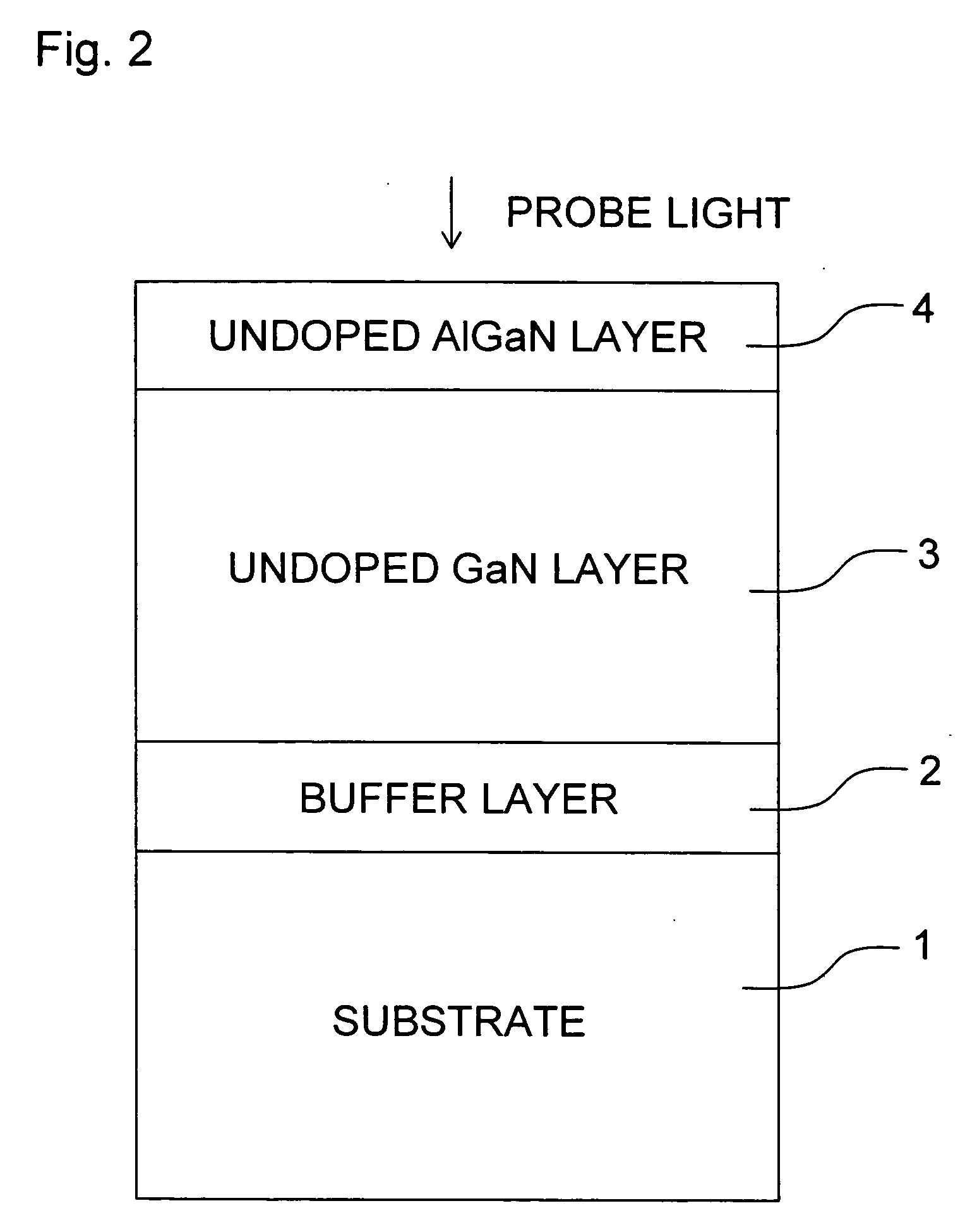
[0051]FIG. 1 shows a flow chart of a method for evaluating a surface, according to the present invention. Herein exemplified is, for a typical sample, a nitride semiconductor epitaxial wafer which has a HEMT (high electron mobility transistor) structure consisting of buffer layer 2, undoped GaN layer 3 and undoped AlGaN layer 4 are sequentially grown on substrate 1, as shown in FIG. 2.
[0052] First, in step a1 of FIG. 1, the surface of the undoped AlGaN layer 4, which is located at an uppermost layer of the sample, is irradiated with probe light. Next, in step a2, an optical reflection spectrum peculiar to an exciton in the undoped AlGaN layer 4 is measured.
[0053] For a method of measuring the reflection spectrum, a) monochromatic light is used for the probe light, and then a change of intensity of reflected light from the sample is measured while changing the wavelength of the probe light, or b) continuous spectrum light is used for the probe light, and then the reflection spectru...
embodiment 2
[0069]FIG. 4 is a block diagram showing an example of an surface evaluating apparatus according to the present invention. The surface evaluating apparatus includes light source 11, spectroscope 12, sample stage 21, detector 2, and computer 50.
[0070] The light source 11 generates light with the continuous spectrum that covers a wavelength range required for spectrum measurement. The spectroscope 12 disperses the light with the continuous spectrum from the light source 11 to output monochromatic probe light. The wavelength of the probe light can be changed continuously according to a control signal from the computer 50. The probe light from the spectroscope 12 is focused onto the measurement area of the sample S with a desired spot size.
[0071] The sample stage 21 holds the sample S so as to adjust the three-dimensional position (X-Y-Z directions) or angles (pitch, yaw and roll) of the sample S using adjusting mechanism 22. The adjusting mechanism 22 may be manually operated or be op...
embodiment 3
[0079]FIG. 5 is a block diagram showing another example of an surface evaluating apparatus according to the present invention. The surface evaluating apparatus includes light source 11, sample stage 21, spectroscope 35, multi-channel detector 36, and computer 50.
[0080] The light source 11 generates probe light with the continuous spectrum that covers a wavelength range required for spectrum measurement. The probe light is focused onto the measurement area of the sample S with a desired spot size.
[0081] The sample stage 21 holds the sample S so as to adjust the three-dimensional position (X-Y-Z directions) or angles (pitch, yaw and roll) of the sample S using adjusting mechanism 22. The adjusting mechanism 22 may be manually operated or be operated according to a control signal from the computer 50.
[0082] The light reflected from the sample S is collected S into the spectroscope 35 by condenser lens 31, and then inputted to the multi-channel detector 36. The spectroscope 35 is con...
PUM
 Abstract
Description
Claims
Application Information