
Surface acoustic wave device and method of manufacturing the same

Active Publication Date: 2007-05-10
NDK SAW DEVICES CO LTD
View PDF9 Cites 33 Cited by
  • Summary
  • Abstract
  • Description
  • Claims
  • Application Information

AI Technical Summary

Benefits of technology

[0056] The objects of the present invention is to provide a surface acoustic wave device provided with a pseudo-single crystal aluminum electrode film which is excellent in power durability, easily manufactured and can be grown with good reproducibility, and a method of manufacturing thereof.
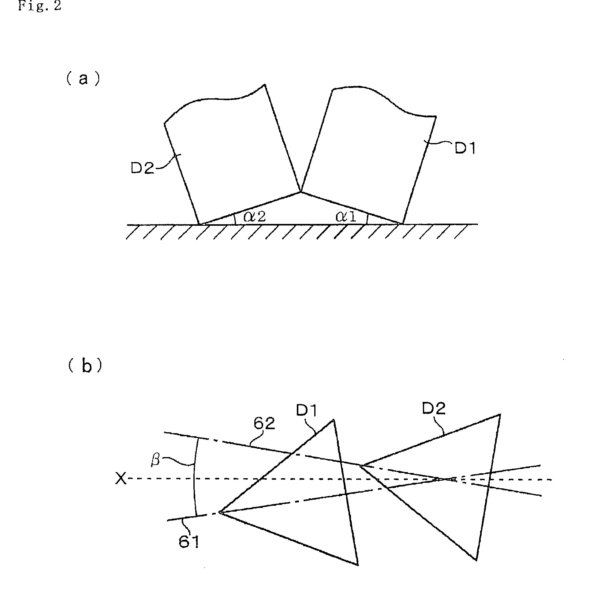
[0058] Then, the present inventors studied a growth process of an aluminum film growing on a titanium buffer film, using a piezoelectric substrate to which only a cleaning process by, for instance, ultrasonic cleaning to wash off a stain on the substrate surface is given while a substrate preprocessing process by wet etching or the like of the piezoelectric substrate is omitted, and the thickness of the titanium buffer film is varied. As a result, the present inventors have discovered a growth mode existing in a form never reported before, and appearing with good reproducibility, which leads to accomplishment of the present invention. The aluminum film manufactured according to this new growth mode is a so-called pseudo-single crystal aluminum film composed of two (111) domains, not a single crystal film having a single growth direction, nor a twin structured film having a plurality of centers of symmetry. The pseudo-single crystal aluminum film has the following characteristics.
[0077] According to the present invention, since an aluminum electrode layer or an aluminum alloy electrode layer formed on a piezoelectric substrate is a pseudo-single crystal composed of two (111) domains, of which displacement of the azimuth angle is within 15°, it shows excellent power durability. Since the electrode of the present invention does not require preprocessing of the substrates such as wet etching or the like for removal of a deteriorated layer created by processing the disordered crystal structure of the substrate surface, the electrode can be manufactured easily, and since a pseudo-single crystal aluminum electrode film in which two (111) single crystal domains grow separately can be grown with good reproducibility, the surface acoustic wave device excellent in power durability can be manufactured at low costs with a high production yield.

Problems solved by technology

Therefore, it is considered to be difficult to grow a single crystal aluminum film with good reproducibility.

Method used


Image

  • Surface acoustic wave device and method of manufacturing the same
  • Surface acoustic wave device and method of manufacturing the same
  • Surface acoustic wave device and method of manufacturing the same

Examples


embodiment 1

[0112] A 40 degree Y-cut LiTaO3 substrate was immersed in an organic solvent, such as isopropyl alcohol (IPA), and ultrasonic cleaning was carried out by applying ultrasonic into the solution. Then, the substrate was put into a DC magnetron sputtering apparatus. After vacuum exhausting to 5×10⁻⁸ Torr, a high purity argon (Ar) gas was introduced into the apparatus via a mass flow controller, and 10 nm of titanium (Ti), and 200 nm of aluminum (Al) were deposited in sequence. For any targets, deposition was conducted under conditions of argon pressure 7 mTorr, and DC 0.5 A. Note that the substrate temperature was kept at room temperature.

[0113] Both (111) and (200) pole figures of this aluminum film were measured using a 4-axis X-ray diffractometer with CuKα as an X-ray source. Diffraction angles of 111 reflection and 200 reflection (2 θ) are 38.5° and 44.8° respectively. The sample was set to an X-ray diffractometer (goniometer stage) so that the X-axis of a 40 degree Y-cut LiTaO3 su...

embodiment 2

[0117] As a second embodiment, growth on a 40 degree Y-cut LiTaO3 substrate will be explained. In the present embodiment, a titanium (Ti) / aluminum (Al)—0.5 wt % copper (Cu) laminated film was deposited using an ion beam sputtering apparatus. Similarly to embodiment 1, a 36 degree Y-cut lithium tantalate substrate was introduced in the ion beam sputtering apparatus after ultrasonic cleaning with isopropyl alcohol (IPA). Argon ions extracted from a Kaufmann type ion source were irradiated to a target, and the target material sputtered from there was deposited on the substrate. A titanium was deposited under conditions of beam voltage 1000 V, and beam current 30 mA, and aluminum (Al)—0.5 wt % copper (Cu) was deposited under conditions of beam voltage 1200 V, and beam current 50 mA. The respective film thickness were 5 nm and 200 nm. Argon pressure was 2×10⁻⁴ Torr. The substrate temperature was room temperature.

[0118] An aluminum pole figure will be shown in FIG. 11. That it is a pseud...

embodiment 3

[0120] As a third embodiment, growth on a 50 degree Y-cut LiTaO3 substrate will be explained. A titanium (Ti) / aluminum (Al)—0.5 wt % copper (Cu)—3.5 wt % magnesium (Mg) laminated film was deposited using an ion beam sputtering apparatus under the same conditions as those in Embodiment 2. The thickness of titanium (Ti), aluminum (Al)—0.5 wt % copper (Cu)—3.5 wt % magnesium (Mg) are 10 nm and 200 nm respectively.

[0121] An aluminum (111) pole figure is shown in FIG. 12. Assuming that the spots serving as the centers of two (111) domains are A and B, as for the matching relation in the direction vertical to the plane, the axis vertical to the (111) plane is tilted 6 degrees or 9 degrees to the lithium tantalate substrate surface, because the respective coordinates are (Phi, Psi)=(157°, 6°) and (239°, 9°). Meanwhile, since the X-axis of the lithium tantalate substrate matches with Phi=0° in the in-plane matching relation, the direction of the respective (111) domains are almost parall...


PUM

PropertyMeasurementUnit
Thicknessaaaaaaaaaa
Thicknessaaaaaaaaaa
Angleaaaaaaaaaa

Abstract

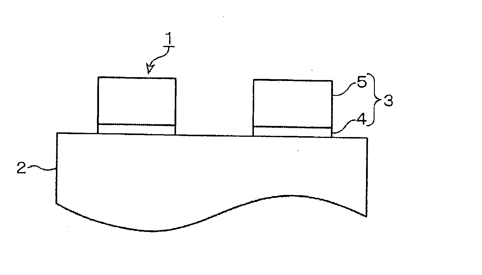
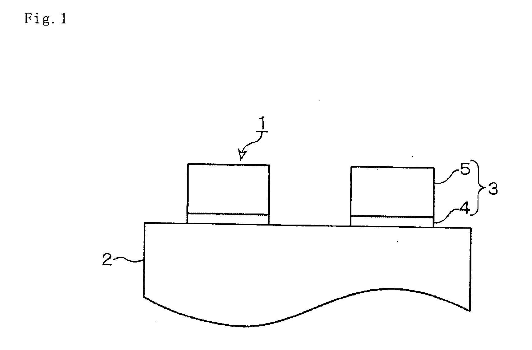
In order to provide a surface acoustic wave device provided with a pseudo-single crystal aluminum electrode film, having excellent power durability, easy to manufacture, and possible to grow with good reproducibility, a titanium buffer film 4 and an electrode film composed of an aluminum film or an aluminum alloy film are formed on a piezoelectric substrate 2 composed of lithium tantalate or lithium niobate. The electrode film 5 comprises a pseudo-single crystal film composed of two (111) domains. Each of the <111> directions of two (111) domains tilts in the range of 0 to 10 degrees to the substrate surface, and the <11-2> directions in the respective (111) domain planes are 1 to 15 degrees apart.

Description

BACKGROUND OF THE INVENTION [0001] 1. Field of the Invention [0002] The present invention relates to a surface acoustic wave device such as a surface acoustic wave filter and a method of manufacturing the same, especially to a surface acoustic wave device electrode. [0003] 2. Description of the Related Art [0004] In recent years, surface acoustic wave devices having the advantages of low insertion loss and small size have been widely used as a resonator or a filter for mobile communication systems. In general, the surface acoustic wave device includes a single crystal piezoelectric substrate (piezoelectric single crystal substrate) and a comb electrode (inter digital transducer, hereinafter referred to as an IDT) formed on the piezoelectric substrate. As a material for the piezoelectric single crystal, quartz, lithium tantalate (LiTaO3), or lithium niobate (LiNbO3), etc. is used, and especially for an RF band filter, a 64 degrees rotated Y-cut LiNbO3 having a large electromechanical...

Claims


Application Information

Patent Timeline
IPC IPC(8): H01L41/047H03H3/08H03H9/145H03H9/25
CPCH03H9/02559Y10T29/42H03H9/14541H03H9/02929
Inventor KAMIJO, ATSUSHI
Owner NDK SAW DEVICES CO LTD
Learn More