Dielectric layer, composition and method for forming the same
a dielectric layer and composition technology, applied in the direction of coatings, solid-state devices, heat inorganic powder coatings, etc., can solve the problems of easy formation of leakage paths and high leakage currents, and improve surface roughness, so as to achieve low leakage current, high dielectric constant, and high uniformity
- Summary
- Abstract
- Description
- Claims
- Application Information
AI Technical Summary
Benefits of technology
Problems solved by technology
Method used
Image

Examples
first embodiment
The First Embodiment
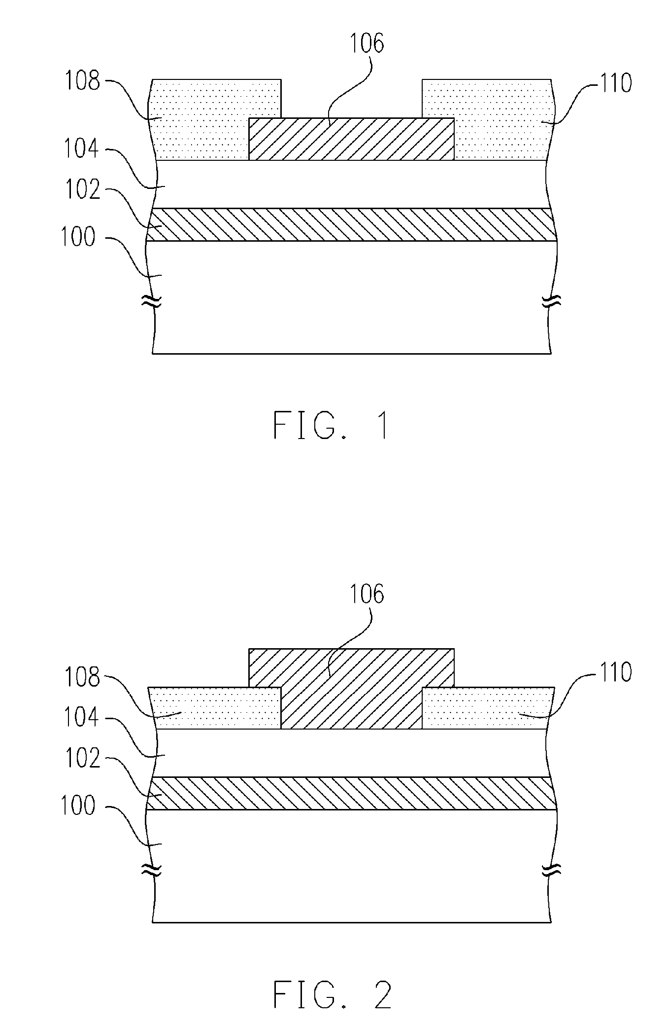
[0035] Referring to FIG. 1, the composition, formed by mixing the 20 wt. % Ta(OC2H5)4, 6 wt. % polyimide and N-methylpyrrolidone (NMP) or r-butyrolactone, is spin coated on the glass substrate with bottom electrode of ITO thereon by speed of 400 rpm / 10 s and 1000 rpm / 30 s, so as to form a thin film. Next, the thin film is performed a soft baking process on the hart plate at 80° C., then, the thin film is performed a hard baking process in an oven at 150° C. to form a gate dielectric layer. Thereafter, a patterned semiconducting layer, a source and a drain are formed, so as to complete a transistor with top contact structure. Thereafter, I-V and C-V characteristics of the transistor are measured. The dielectric constant is 5.7. The mobility is 0.047 cm2 / Vs. The on / off ratio is 104-105.
second embodiment
The Second Embodiment
[0036] The transistor with top contact structure is formed according to the aforementioned method, besides, the composition is changed to the compound formed by 30 wt. % Ta2(acac)5, 6 wt. % polyimide and N-methylpyrrolidone (NMP) or r-butyrolactone. I-V and C-V characteristics of the transistor are measured. The dielectric constant is 6.7. The mobility μ is 0.059 cm2 / Vs. The on / off ratio is 104.
[0037] The organometallic compound in the aforementioned composition is described by the example of tantalum alkoxide. The other metal alkoxide of the present invention can also form the composition using the methods similar to the first or second embodiment, wherein the metal includes Al, Ti, Zr, Ta, Si, Ba, Ge or Hf, and, after baking the formed composition, the dielectric layer can be formed.
PUM
| Property | Measurement | Unit |
|---|---|---|
| Temperature | aaaaa | aaaaa |
| Temperature | aaaaa | aaaaa |
| Temperature | aaaaa | aaaaa |
Abstract
Description
Claims
Application Information
 - R&D
- Intellectual Property
- Life Sciences
- Materials
- Tech Scout
- Unparalleled Data Quality
- Higher Quality Content
- 60% Fewer Hallucinations
Browse by: Latest US Patents, China's latest patents, Technical Efficacy Thesaurus, Application Domain, Technology Topic, Popular Technical Reports.
© 2025 PatSnap. All rights reserved.Legal|Privacy policy|Modern Slavery Act Transparency Statement|Sitemap|About US| Contact US: help@patsnap.com