

Short-wavelength polarizing elements and the manufacture and use thereof
a polarizing element and short-wavelength technology, applied in the field of short-wavelength polarizing elements, can solve the problems of ineffective ultraviolet light polarizers, large installation space within the exposure apparatus, and large deflection of prism-type elements
- Summary
- Abstract
- Description
- Claims
- Application Information
AI Technical Summary
Benefits of technology
Problems solved by technology
Method used
Image

Examples
example 1
[0099] Polyimide (Durimide™ 285, Arch Chemicals, Inc., diluted to 3 wt % in gamma-butyrolactone) was spin coated at 1500 rpm for 45 seconds onto a 4-inch-diameter amorphous quartz wafer (AQ: Asahi Glass Co., Ltd.) to form an organic polymer layer. The resulting film, 100 nm thick, was then heated at 90° C. for 30 minutes, and at 150° C. for another 30 minutes, to evaporate residual solvent and crosslink the polymer.
[0100] Next, silicon nitride was deposited using plasma-enhanced chemical vapor deposition. The deposition was performed at 150 sccm of N2, 110 sccm of SiH4 / N2 and 2 sccm of NH3 maintained at 900 mTorr, ignited with 20 W (80 mW / cm2) and lasting 75 seconds, for a final silicon nitride layer thickness of 22 nm. This inorganic substance layer serves an etch barrier in subsequent processing.
[0101] Next, a film of polystyrene-poly(n-hexylmethacrylate) diblock copolymer was deposited by spin-coating from a 1 wt % solution in toluene, at 2500 rpm for 45 seconds. The molecular ...
example 2
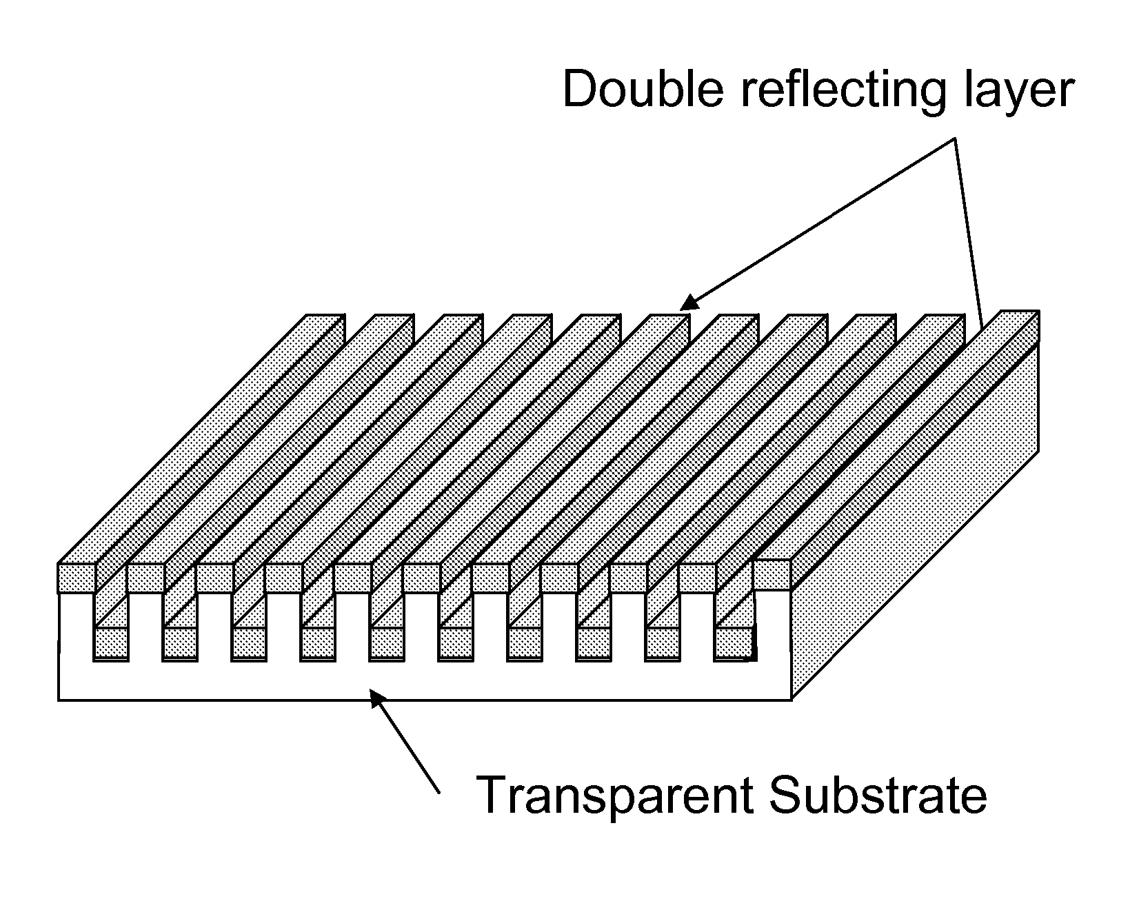
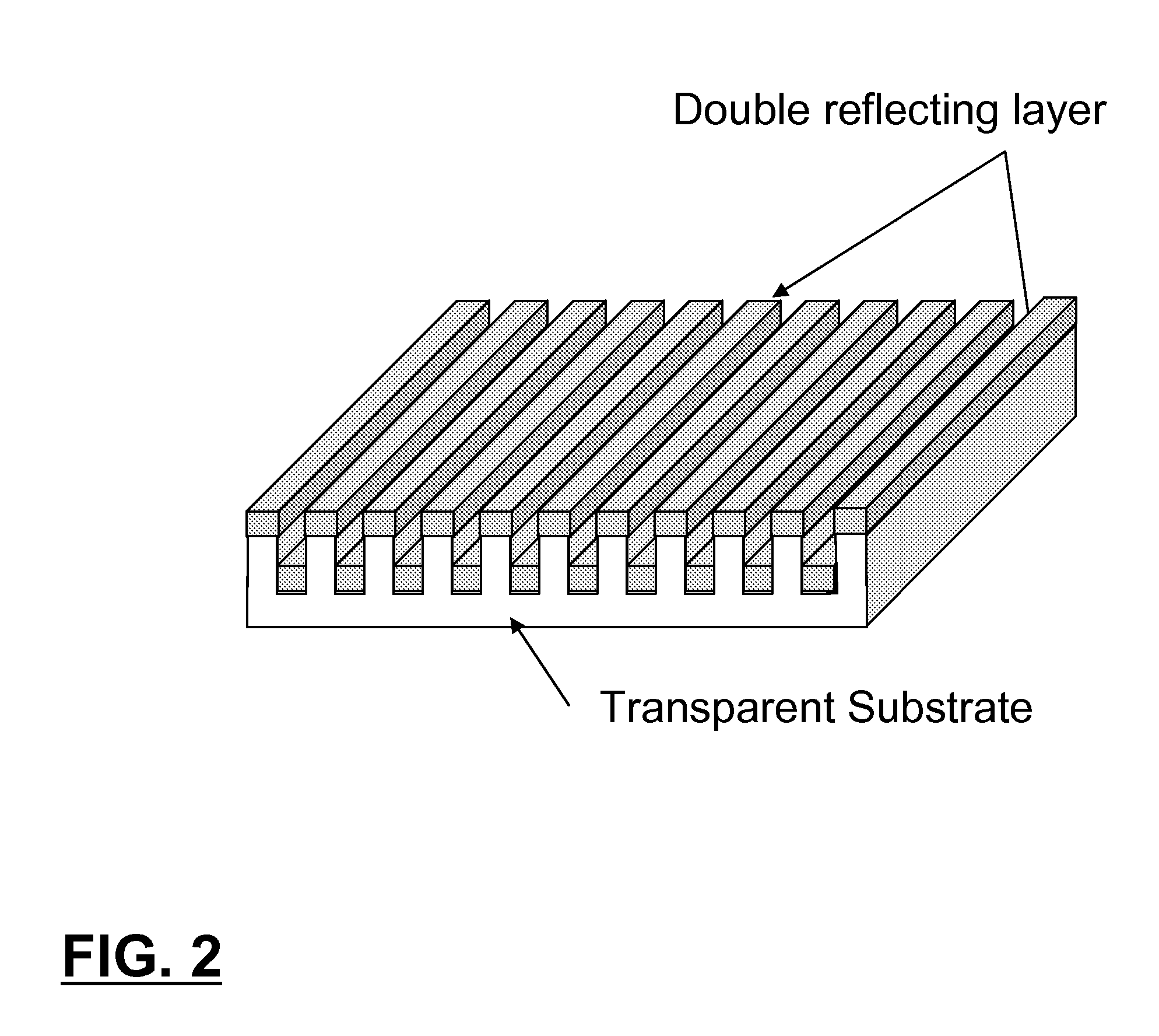
Double Layer Polarizer
[0106] In this example, the same process was done as in Example 1 until the O2 RIE. Then, the amorphous quartz wafer was etched using CF4 RIE, at 10 sccm, 15 m Torr pressure, and 100 W of RF power (0.4 W / cm2) for 50 seconds. The amorphous quartz was engraved 70 nm as a pattern of ridges located beneath the original locations of the polystyrene cylinders.
[0107] All of the organic substances were removed by immersing the assembly in 1-methyl-2-pyrrolidinone and sonicating for three times, and by oxygen plasma ashing.
[0108] Aluminum was then deposited onto the resulting striped pattern using an electron-beam evaporator, for an aluminum film thickness of 40 nm, to complete the double layer polarizer.
example 3
Finer Stripe Pattern Manufactured by Metal Staining Method
[0109] In this example, 3 wt % propyleneglycol monomethylether acetate (PGMEA) solution of poly(4-hydroxystyrene) (ALDRICH) was spin coated at 2000 rpm for 45 seconds onto a 4-inch-diameter amorphous quartz wafer to form an organic polymer layer. The resulting film, 80 nm thick, was then heated at 120° C. for 90 seconds to evaporate residual solvent.
[0110] Next, silicon was deposited using an electron-beam evaporator and the resulting thickness was 10 nm. Then, a film of polystyrene-poly(ethylene-alt-propylene) diblock copolymer was deposited by spin-coating from a 0.75 wt % solution in toluene, at 2500 rpm for 45 seconds. The molecular weight of the polystyrene block was 5,000 g / mol and that of the poly(ethylene-alt-propylene) block was 13,000 g / mol, so that the morphology of the film involved cylinders of polystyrene in a matrix of poly(ethylene-alt-propylene), with a period of 16 nm. The resulting thickness of the block ...
PUM
| Property | Measurement | Unit |
|---|---|---|
| wavelengths | aaaaa | aaaaa |
| wavelengths | aaaaa | aaaaa |
| length | aaaaa | aaaaa |
Abstract
Description
Claims
Application Information