
Solar cell and method of fabricating the same

a technology of solar cells and insulating films, applied in the field of solar cells, can solve the problems of poor passivation effect, small reflection loss, low conversion efficiency , etc., and achieve the effect of reducing the substrate temperature and improving the passivation characteristic of the insulating film

Inactive Publication Date: 2007-08-16
SHIN ETSU CHEM IND CO LTD
View PDF6 Cites 81 Cited by
  • Summary
  • Abstract
  • Description
  • Claims
  • Application Information

AI Technical Summary

Benefits of technology

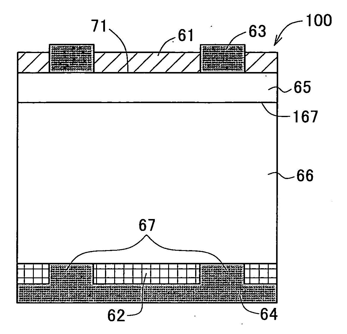
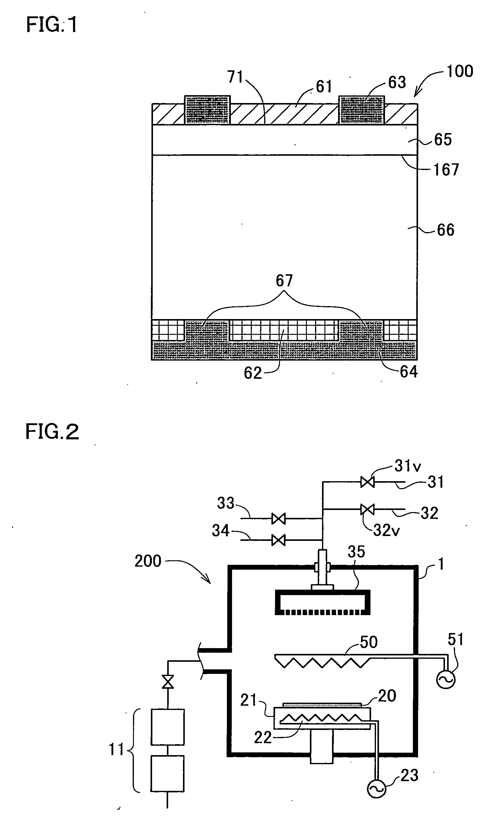
[0018] According to the first aspect of this invention, the light-receiving-surface-side insulating film is configured using a silicon-base insulating film having a large dielectric constant and being capable of providing a desirable passivation effect, and is also configured as a low-hydrogen-content inorganic insulating film, having a hydrogen content of less than 10 at %, so that the durability of the light-receiving-surface-side insulating film against ultraviolet radiation can be improved to a large degree. More specifically, the passivation effect of the insulating film is less likely to cause time-dependent degradation even if the solar cell is used under an environment in which a light having a large energy content of ultraviolet radiation such as a sunray and a fluorescent lamp is irradiated for a long duration of time, and the conversion efficiency η can be maintained at a desirable value for a long period.
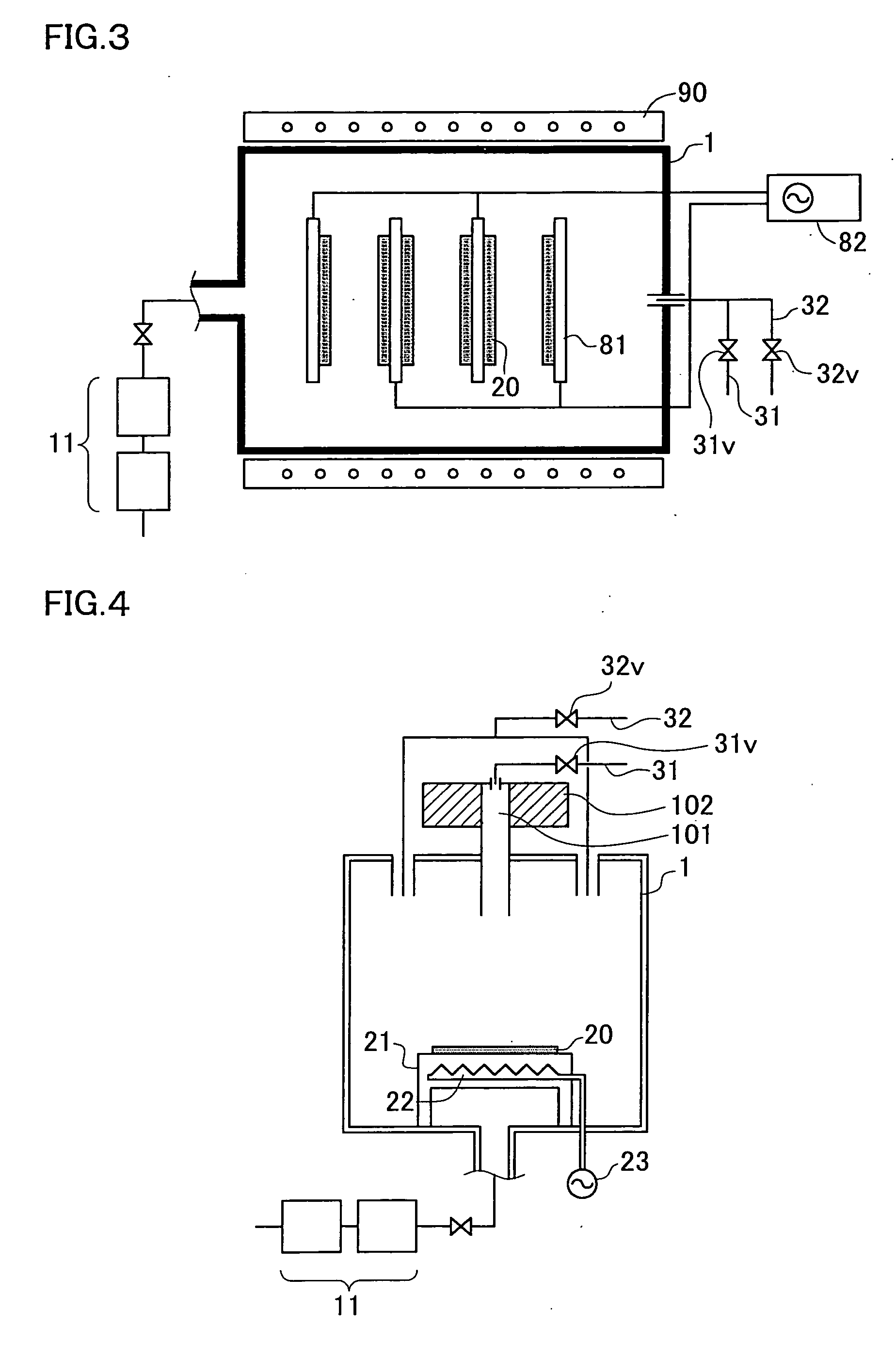
[0043] The present inventors found that the passivation characteristic of the insulating film can further be improved by surface-treating the inorganic insulating film, after. being deposited, by supplying the post-treatment gas to the surface thereof, while allowing the post-treatment gas to cause catalytic decomposition reaction with the aid of the heat catalyst, similarly to as in the above-described surface treatment. It is to be noted that the post-treatment after the film formation, proceeded in a hydrogen atmosphere under heating without using any catalyst, has already been known as hydrogen annealing, whereas the catalyst-assisted method of this invention is far superior thereto in the passivation effect. This is supposedly because decomposition chemical species are intentionally produced by the catalytic reaction in the process chamber, and the decomposition chemical species can diffuse into the insulating film to thereby terminate the dangling bonds. According to this method, it is also allowable to lower the substrate temperature than in the general hydrogen annealing, and this raises another advantage of ensuring a more stable post-treatment as compared with the hydrogen annealing, without impairing contact characteristic between the electrodes and the substrate.

Problems solved by technology

In this process, some of the carriers which could possibly be extracted as current may be lost through interface states which reside in the substrate surface other than electrode surfaces, and this may lower the conversion efficiency η.
Silicon oxide film has long been used as this sort of insulating film, but the refractive index of which is as small as 1.4 or around, and causes a slightly large reflection loss when used on the light-receiving-surface-side.
The plasma CVD is widely applied to processes of fabricating solar cells because it can ensure a relatively high deposition rate even under a substrate temperature of relatively as low as 400° C. The process, however, raises a problem in that high-energy charged particles produced in the plasma are highly causative of damages of the deposited film or the surface of the substrates (so-called plasma damage), so that the obtained silicon nitride film tends to have a large interface state density, and consequently results in only a poor passivation effect.
A large shift in the film composition towards the silicon-excessive side causes effluence of electrons produced by anion deficiency towards the semiconductor substrate so as to produce positive fixed charge on the cation side, and this results in band bending.
This structure, however, suffers from large drawbacks as described below.
However, such desirable passivation cannot be obtained anyhow, because it is difficult to suppress damage by the general plasma CVD.

Method used


Image

  • Solar cell and method of fabricating the same
  • Solar cell and method of fabricating the same
  • Solar cell and method of fabricating the same

Examples


experiment 1

[0070] A 3-inch circular (100) single crystal silicon substrate (FZ method, B doped) having a resistivity of 1.5 Ωcm was cleaned with 2% hydrofluoric acid for 1 minute, rinsed with ultra-pure water for 5 minutes, and dried by blowing a dry nitrogen. Thereafter a silicon nitride film of 80 nm thick, having a refractive index of 2.4 (Si / N atomic ratio=1.48: without hydrogen dilution), was formed on both surfaces thereof by the catalytic CVD process. Next, an effective lifetime was measured using a lifetime scanner while irradiating a white bias light of 0.5 sun, and the surface recombination velocity was calculated on the basis of a result of lifetime measurement of the same substrate but subjected to chemical passivation (iodine / ethanol treatment). On the other hand, using a 400-W metal halogen lamp as a light source, one surface of the sample was exposed to ultraviolet radiation, from which wavelength component of 320 nm or shorter is cut by a filter, for 32 hours and 128 hours, and...

experiment 2

[0071] The silicon substrate was cleaned and dried according to the procedures similar to as described in Experiment 1, and by the catalytic CVD process, the substrate was surface-treated using ammonia gas, on both surfaces of which the silicon nitride film having a refractive index of 2.4 was deposited, and then a similar measurement was carried out.

experiment 3

[0072] The silicon substrate was cleaned and dried according to the procedures similar to as described in Experiment 1, and by the catalytic CVD process, the substrate was surface-treated using ammonia gas, on both surfaces of which the silicon nitride film having a refractive index of 2.4 was deposited, post-treated using hydrogen gas, and then a similar measurement was carried out.


PUM


Abstract

A solar cell (100) comprising a semiconductor solar cell substrate (66) having a light receiving surface formed on the first major surface and generating photovoltaic power based on the light impinging on the light receiving surface, wherein the light receiving surface of the semiconductor solar cell substrate (66) is coated with a light receiving surface side insulating film (61) composed of an inorganic insulating material where the cationic component principally comprising silicon, and the light receiving surface side insulating film (61) is a low hydrogen content inorganic insulating film containing less than 10 atm % of hydrogen. A solar cell having an insulating film exhibiting excellent passivation effect insusceptible to aging can thereby be provided.

Description

BACKGROUND OF THE INVENTION [0001] 1. Field of the Invention [0002] This invention relates to a solar cell capable of directly converting light energy to electric energy, and a method of fabricating the same. [0003] 2. Description of the Related Art [0004] A solar cell is a semiconductor element capable of converting light energy into electric power, known types of which include p-n junction type, PIN type and Schottky type, among which the p-n junction type is widely used. It is also possible to roughly classify the solar cell into three types, based on materials composing the substrate, such as silicon crystal-base solar cell, amorphous-silicon-base solar cell and compound-semiconductor-base solar cell. The silicon-crystal-base solar cell is further classified into single-crystal-base solar cell and polycrystal-base solar cell. The silicon-crystal-base solar cell is most disseminated, because silicon crystal substrate for producing the solar cell can be fabricated in a relatively ...

Claims


Application Information

Patent Timeline
IPC IPC(8): H01L31/00H01L21/318H01L31/0216H01L31/04H01L31/068H01L31/072H01L31/18
CPCH01L31/02167H01L31/1804Y02E10/547H01L31/068H01L31/0682H01L31/1868Y02P70/50H01L31/04H01L31/18
Inventor TAKAHASHI, MASATOSHIOHTSUKA, HIROYUKIMATSUMURA, HIDEKIMASUDA, ATSUSHIIZUMI, AKIRA
Owner SHIN ETSU CHEM IND CO LTD
Learn More