This helps you quickly interpret patents by identifying the three key elements:
Problems solved by technology
Method used
Benefits of technology
Benefits of technology
[0019]According to the above-mentioned structure, the nitride semiconductor single crystal having good crystallinity can be grown without the 3C—SiC layer on the Si substrate.
[0021]Thus, the crystallinity of the nitride semiconductor single crystal can be further improved by forming the super-lattice structure of GaN and AlN.
[0022]As described above, according to the present invention, the single crystal film of GaN or AlN having good crystallinity can be obtained with a thickness of one μm or more without the 3C—SiC layer on the Si substrate.
[0023]Further, the crystallinity of the nitride semiconductor single crystal can be further improved by forming the super-lattice structure of GaN and AlN.
[0024]Therefore, the nitride semiconductor single crystal in accordance with the present invention can be used suitably for a light emitting diode, a laser diode, and an electronic diode that can be operated at a high temperature, as well as a high frequency device, thus improving element functions of these.
Among the substrates used conventionally, as compared with Si substrates, large diametersapphire (0001) and 6H—SiC (0001) are difficult to manufacture and their costs are high.
However, in the case of nitride films grown on the Si substrate, since cracks are formed in the nitride films due to a difference of thermal expansion coefficient between Si and nitride films and many crystal defects generate because of a difference of lattice constant between Si and nitride films, it has been difficult to grow a single crystal film having a thickness of one μm or more.
However, cracks are often generated on the Si (111) substrate, when the 3C—SiC (111) layer is grown as a film having a thickness of one μm or more.
Additionally, in a high frequency device, if its operational frequency is high, an eddy current generates in the substrate and then Joule heat leads to trouble with device operation, so that an insulating substrate is required.
On the other hand, since 3C—SiC employed as the buffer layer has electric conductivity, the substrate with the 3C—SiC layer is unsuitable as the high frequency device.
Method used
Image
Click on the blue label to locate the original text in one second.
Reading with bidirectional positioning of images and text.
Examples
example 1
[0043]A Si (110) substrate was placed at a growth area in a reaction chamber, and then the Si (110) substrate was heated up to 1100° C. while supplying hydrogen as a career gas for the substrate cleaning.
[0044]Then, with the substrate temperature held, trimethyl aluminum (TMA) and ammonia were supplied as aluminum and nitrogen sources, respectively and a 2H—AlN buffer layer with a thickness of 10-500 nm was grown on the above-mentioned Si (110) substrate.
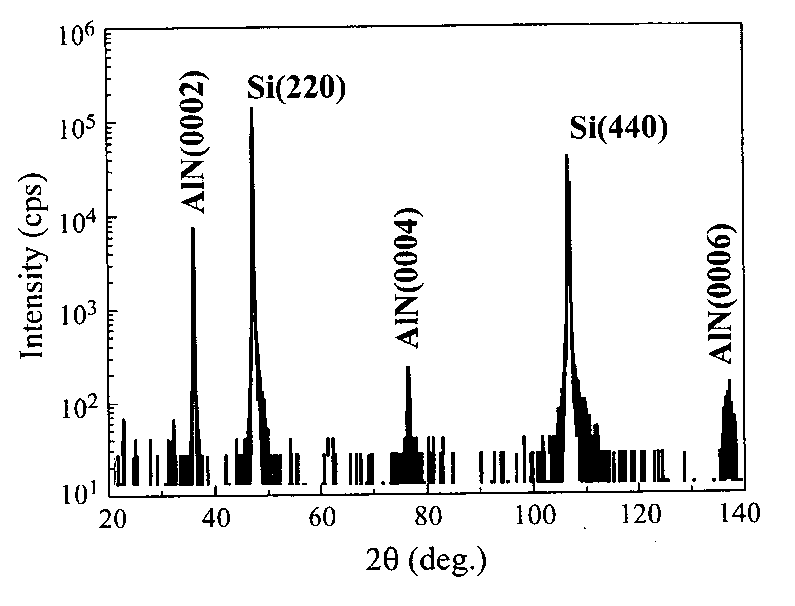
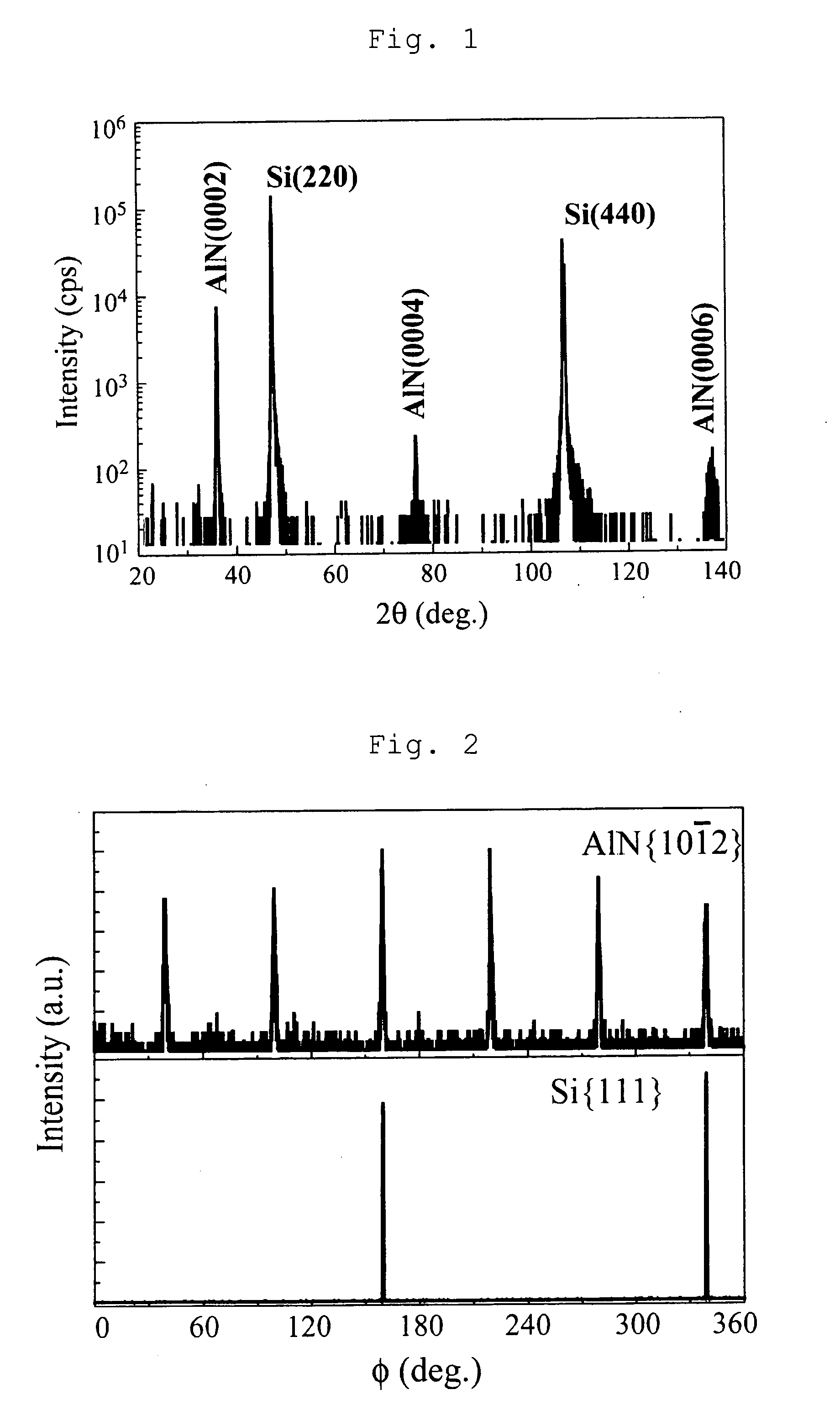
[0045]The 2H—AlN buffer layer grown on this Si (110) substrate was examined by θ-2θ scan and φ scan of X raydiffraction, and the orientations of the film in a growth direction (thickness direction) and in its plane were evaluated. These measured spectra are shown in FIGS. 1 and 2, respectively.
[0046]As shown in FIG. 1, it was confirmed that the growth direction of AlN film as the buffer layer was orientated with respect to the normal direction of Si (110) substrate.
[0047]Further, as shown in FIG. 2, in φ scan of X raydiffraction,...
example 2
[0053]As with Example 1, a 2H—AlN buffer layer was grown on a Si (110) substrate.
[0054]Then, a substrate temperature was increased to 1200° C. or more, TMA and ammonia were supplied as source materials, and an AlN (0001) single crystal layer was grown.
[0055]When the above-mentioned AlN (0001) single crystal layer was grown with the thickness of one μm or more, any cracks were not observed.
example 3
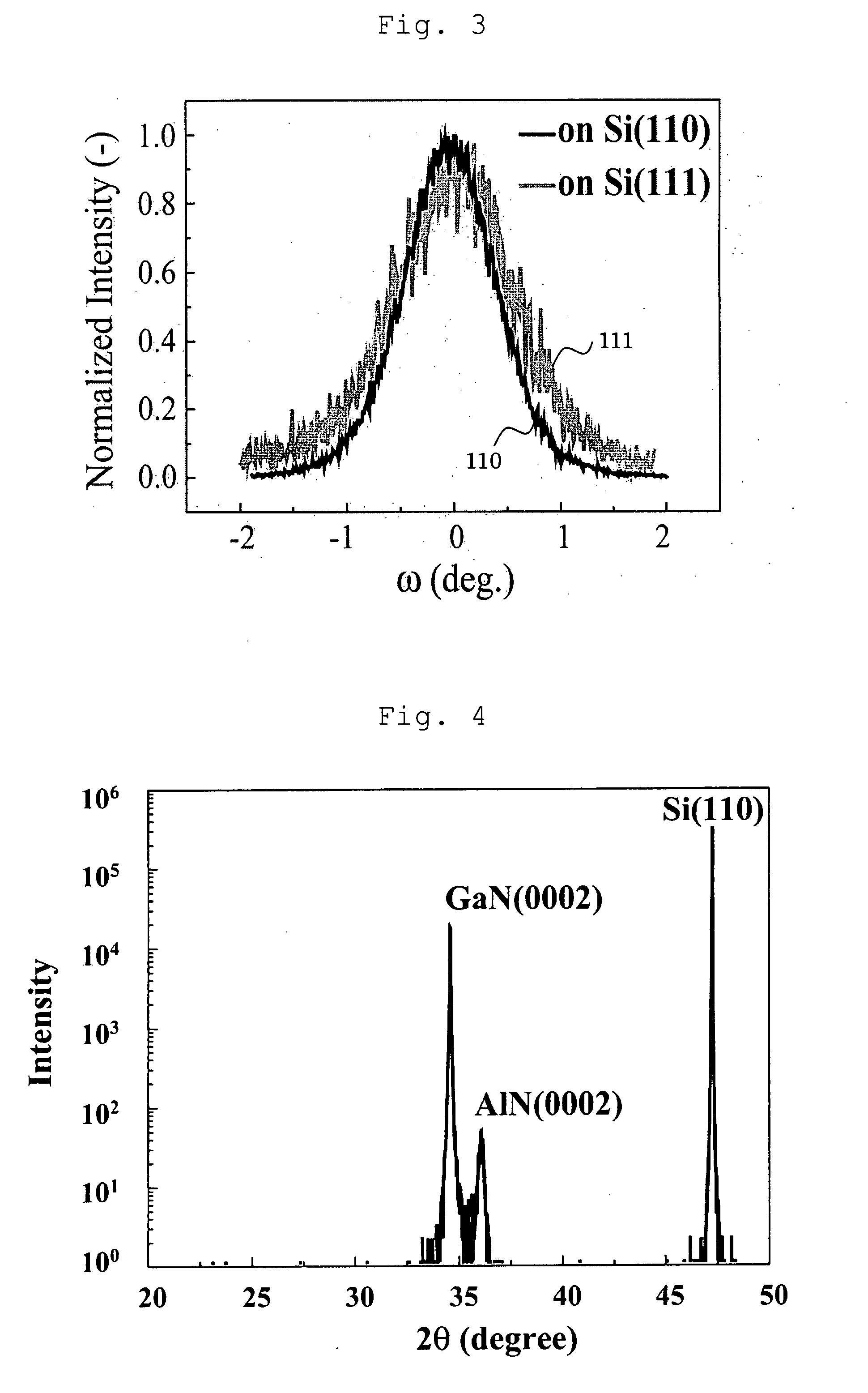
[0060]As with Example 1, a 2H—AlN buffer layer was grown on a Si (110) substrate. Then a substrate temperature was set to be 1000° C., TMG or TMA as a group III source and ammonia as a nitrogen source material were supplied to form 80 pairs of films where one pair films included the GaN (0001) single crystal layer with the thickness of 25 nm and the AlN (0001) single crystal layer with the thickness of 5 nm.
[0061]A GaN (0001) layer was grown thereon, and it was confirmed that a film could be grown with the thickness of two μm or more without a crack generation.
PUM
Abstract
The present invention provides a nitridesemiconductorsingle crystal including galliumnitride (GaN) or aluminum nitride (AlN) which are formed as a film to have good crystallinity without forming a 3C—SiC layer on a Si substrate, and which can be used suitably for a light emitting diode, a laser light emitting element, an electronic element that can be operated at a high speed and a high temperature, etc., as well as a high frequency device.A GaN (0001) or AlN (0001) single crystal film, or a super-lattice structure of GaN (0001) and AlN (0001) is formed on a Si (110) substrate via a 2H—AlN buffer layer.
Description
BACKGROUND OF THE INVENTION[0001]1. Field of the Invention[0002]The present invention relates to a nitride semiconductorsingle crystal including gallium nitride (GaN) and / or aluminum nitride (AlN) which are used suitably for a light emitting diode, a laserdiode, an electronic diode that can be operated at a high temperature, and can be handled at high power and high frequencies.[0003]2. Description of the Related Art[0004]A nitride semiconductor represented by GaN and AlN has a wide band gap and is expected to be a material applicable to a light emitting diode, a laserdiode, an electronic diode that can be operated at a high speed and a high temperature, as a wide band gap semiconductor having outstanding characteristics, such as higher electric breakdown field and larger saturated drift velocity of electrons, etc.[0005]Since the above-mentioned nitride semiconductor has a high melting point and equilibrium vapor pressure of nitrogen is very high, bulk crystal growth from the mel...
Claims
Application Information
Patent Timeline
Application Date:The date an application was filed.
Publication Date:The date a patent or application was officially published.
First Publication Date:The earliest publication date of a patent with the same application number.
Issue Date:Publication date of the patent grant document.
PCT Entry Date:The Entry date of PCT National Phase.
Estimated Expiry Date:The statutory expiry date of a patent right according to the Patent Law, and it is the longest term of protection that the patent right can achieve without the termination of the patent right due to other reasons(Term extension factor has been taken into account ).
Invalid Date:Actual expiry date is based on effective date or publication date of legal transaction data of invalid patent.

