Method for pattern formation

a pattern and pattern technology, applied in nanotechnology, nanotechnology, semiconductor devices, etc., can solve the problems of large fabrication throughput, high cost of lithography in manufacturing process, and difficulty in satisfactorily ensuring the etching resistance of the pattern formed as the mask, etc., to achieve high aspect ratio, simple process, and satisfactory etching resistance

Inactive Publication Date: 2008-02-21
KK TOSHIBA
View PDF27 Cites 68 Cited by
  • Summary
  • Abstract
  • Description
  • Claims
  • Application Information

AI Technical Summary

Benefits of technology

[0015]In view of the above problems of the prior art, the present invention has been made, and an object of the present invention is to provide a method for pattern formation that, in a microfabrication technique using an etchi

Problems solved by technology

Increased fineness of fabrication dimension and increased pattern density, however, have led to huge cost of lithography in the manufacturing process.
This, however, involves a large problem with fabrication throughput.
In general, however, the size in the layer thicknesswise direction of the phase-separated structure of the block copolymer is equal to or smaller than the size of a pattern formed in a two-dimensional direction on the substrate, and, hence, it is difficult to satisfactorily ensure etching resistance of the pattern formed as the mask.
Accordingly, when the object is etched using this phase-separated structure of the block copolymer mask as an etching mask, the fabrication of a structure having a satisfactorily high aspect ratio is impossible.
Also in this method, however, since a high aspect ratio is not obtained in the transfer of the block copolymer onto the pattern transfer film, in some cases, the pattern cannot be faithfully transferred without difficulties.
Unsatisfactory aspect ratio in etchin

Method used


Image

  • Method for pattern formation
  • Method for pattern formation
  • Method for pattern formation

Examples


example 1

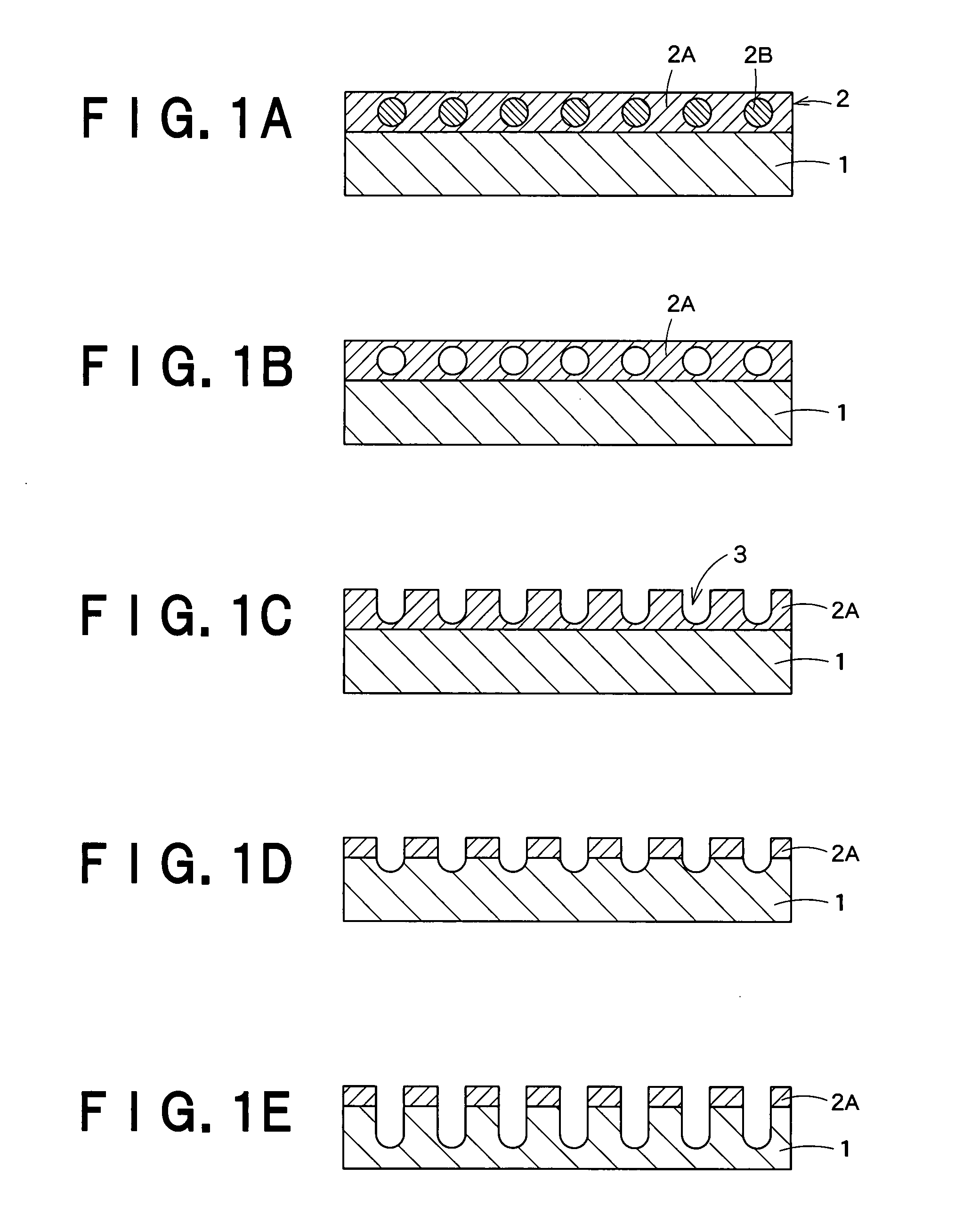
[0050]A diblock copolymer comprising polystyrene (PS) having a molecular weight of 9500 and polyethylene oxide (PEO) having a molecular weight of 9500 was dissolved in diglyme to prepare a 2.5% polymer solution for coating. 125 mg of T-7 (5500T) manufactured by Tokyo Ohka Kogyo Co., Ltd., which is a solution of a methylsiloxane derivative, was added to 250 mg of the polymer solution to give a homogeneous solution.

[0051]The homogeneous solution thus obtained was filtered through a membrane filter having a pore size of 0.5 μm and was coated onto a silicon wafer (a substrate) to a thickness of 30 nm. The coated substrate was placed in a nitrogen atmosphere oven, was heated to 400° C. at a temperature rise rate of 1.5° C. / min, and was held at the temperature for 2 hr.

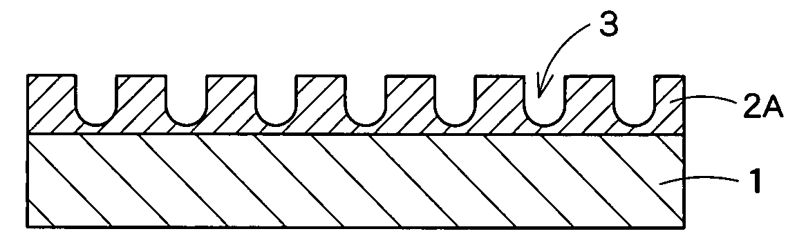
[0052]The cross-section of the baked film thus obtained was observed under TEM. As a result, it was found that about 23 nm-pitch holes were formed. Next, etching with SF6 gas was carried out using the formed pattern as a ma...

example 2

[0053]A film having a microstructure was prepared in the same manner as in Example 1, except that a block copolymer comprising polystyrene (PS) having a molecular weight of 3800 and polyethylene oxide (PEO) having a molecular weight of 6500 was used instead of the block copolymer used in Example 1.

[0054]It was found that, in the baked film thus obtained, 15 nm-pitch holes were formed. In the same manner as in Example 1, the pattern was transferred to the underlying silicon substrate.

example 3

[0055]A film having a microstructure was prepared in the same manner as in Example 1, except that a block copolymer comprising polystyrene (PS) having a molecular weight of 3000 and polyethylene oxide (PEO) having a molecular weight of 3000 was used instead of the block copolymer used in Example 1.

[0056]It was found that, in the baked film thus obtained, 15 nm-pitch cylinders were formed. In the same manner as in Example 1, the pattern was transferred to the underlying silicon substrate.


PUM

PropertyMeasurementUnit
Affinityaaaaaaaaaa

Abstract

There is provided a method for pattern formation, including a step of coating a composition comprising a block copolymer, a silicon compound, and a solvent for dissolving these components onto an object to form a layer of the composition on the object, a step of subjecting the layer of the composition to self-organization of the block copolymer to cause phase separation into a first phase, in which the silicon compound is localized, having higher etching resistance by heat treatment or/and oxygen plasma treatment, and a second phase comprising a polymer phase and having lower etching resistance by heat treatment or/and oxygen plasma treatment, and thereby forming a pattern layer with a fine pattern, and a step of etching the object using as a mask the thus formed pattern layer.

Description

CROSS-REFERENCE TO RELATED APPLICATION[0001]This application is based upon and claims the benefit of priority from the prior art Japanese Patent Application No. 221555 / 2006, filed on Aug. 15, 2006; the entire contents of which are incorporated herein by reference.BACKGROUND OF THE INVENTION[0002]The present invention relates to a method for fabricating a fine pattern that has a periodic array structure and utilizes a self-organizational phase separation structure of a block copolymer.[0003]The method for pattern formation according to the present invention is suitable for use, for example, in the manufacture of high-density recording media and highly integrated electronic components.[0004]A recent rapid improvement in function of information technology equipment such as personal computers relies greatly on advance in microfabrication technology used, for example, in the manufacture of semiconductor devices. Up to now, an attempt to increase the fineness of fabrication dimension has ...

Claims


Application Information

Patent Timeline
IPC IPC(8): C23F1/02
CPCH01L21/3086B82Y10/00Y10S438/942H01L21/0274
Inventor KIHARA, NAOKOHIEDA, HIROYUKI
Owner KK TOSHIBA
Why Eureka
Try Eureka