
Compound semiconductor modified surface by use of pulsed electron beam and ion implantation through a deposited metal layer

a technology of deposited metal layer and modified surface, which is applied in the direction of polycrystalline material growth, crystal growth process, chemistry apparatus and processes, etc., can solve the problems of overly difficult conditions to achieve on a practical scale, slow light energy transfer techniques such as flash lamps, and undesirable temperature rise in the entire substra

Inactive Publication Date: 2008-04-17
MELAS ANDREAS A
View PDF12 Cites 21 Cited by
  • Summary
  • Abstract
  • Description
  • Claims
  • Application Information

AI Technical Summary

Problems solved by technology

For example, in the case of GaN, at the extrapolated melting point of 2518 C., the partial pressure of Nitrogen over the liquid GaN is approximately ten thousand atmospheres (Reference #5), an exceedingly difficult condition to achieve on a practical scale.
Given that these compound semiconductors are sensitive and prone to decomposition at higher than ambient temperatures, any technique which must improve the crystal quality needs to be very fast and below the time it takes to break apart a molecular bond, or typically below a microsecond.
Light energy transfer techniques such as from a flash lamp are slow compared to a pulsed electron beam and produce undesirable temperature rise in the entire substrate.
At the other extreme such as when the pulsed electron beam is highly focused, it can lead to very rapid and localized temperature rise and thus to vaporization and consequently deposition of the target material on a substrate (Reference #6).
However this is the opposite process and not as likely to lead to a single crystalline material, particularly for compound semiconductors which do not have a defined melting point and may decompose on heating.
In this unique combination, the metal caps the material during the high temperature produced by exposure to the pulsed electron beam, and does not allow it to decompose.
A particularly difficult problem for these materials relates to the substrate necessary to grow thin layers that comprise the laser, L.E.D or other electronic or optoelectronic device (Reference 3).
It is known that the growth of large (over a few mm in diameter) single crystal substrates, is extraordinarily difficult to achieve compared to GaAs or InP, for example, which are commercially available to 150 mm Outside Diameter (OD).

Method used


Image

  • Compound semiconductor modified surface by use of pulsed electron beam and ion implantation through a deposited metal layer
  • Compound semiconductor modified surface by use of pulsed electron beam and ion implantation through a deposited metal layer
  • Compound semiconductor modified surface by use of pulsed electron beam and ion implantation through a deposited metal layer

Examples


example 1

Pulsed Electron Beam Through Deposited Aluminum Layer

[0026] A. Deposit a high purity layer of Aluminum metal in the range of 0.01 to several micrometers thick. This can be by ebeam evaporation or by a Chemical Vapor Deposition or other technique, as long as high purity is achieved. The use of Aluminum is significant not only because it is a Group III metal and highly conductive but also because AlxGa1-xN layer alloy can be produced. At concentrations below about 1 atomic percent, the Aluminum will not alter significantly the material properties of GaN.

[0027] B. Use a pulsed electron beam as wide as 100 mmOD, generated by capacitor discharge. Typically, an electric field of approximately 10 to 100 KiloVolt is used, a total of 1-50 Kilo Amperes, with a pulse width under a microsecond, typically of 80 to 500 nanoseconds, resulting in an energy fluence from 0.1 to 10 Joules per cm2. The electron beam pulse may be repeated as necessary to optimize the results.

[0028] C. The result of t...

example 2

Pulsed Electron Beam Through Deposited Indium Layer

[0031] A variation of Example 1 is where Indium metal is used instead of Aluminum. This is particularly important since in this case, the resulting InxGa1-xN layer, which has a larger crystal lattice further improves the GaN crystal structure by expansion.

example 3

Pulsed Electron Beam Through Deposited Boron Layer on Group III-Nitride

[0032] Another variation of Example 1 is to use Boron which has the advantage to produce a better metal contact due to the higher energy bandgap than Gallium Nitride itself.


PUM

PropertyMeasurementUnit
partial pressureaaaaaaaaaa
pressureaaaaaaaaaa
Outside Diameteraaaaaaaaaa

Abstract

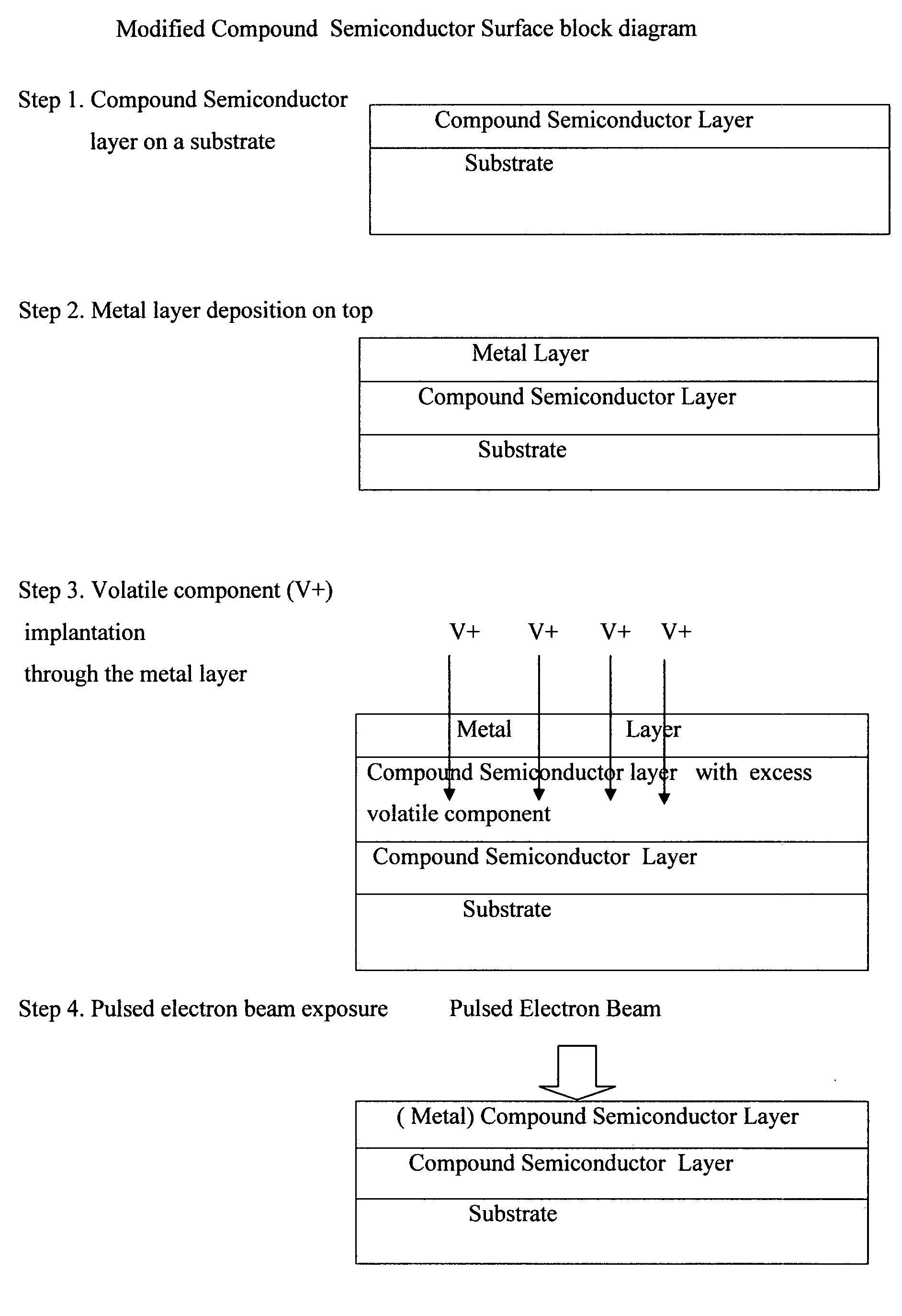
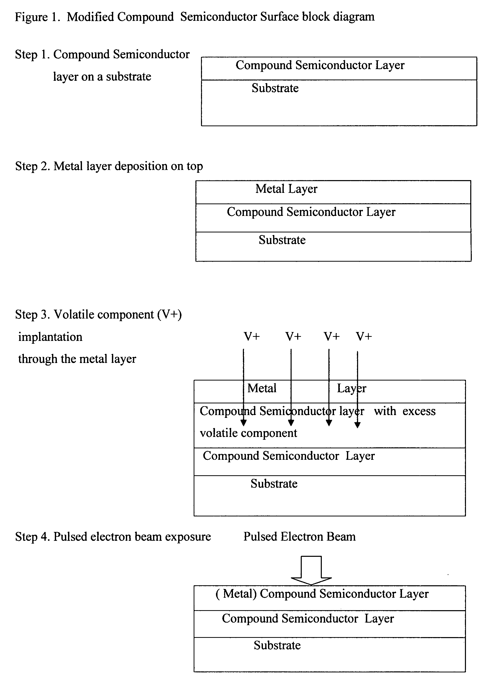
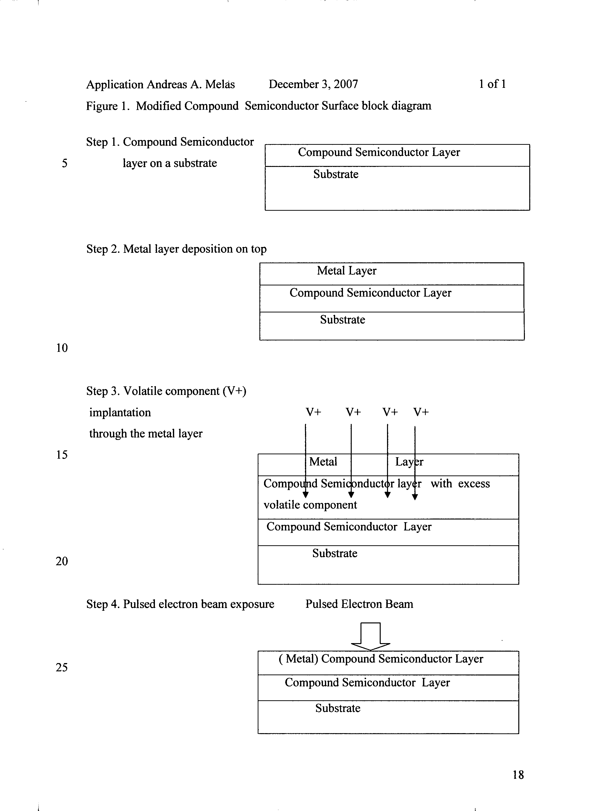
Thermally sensitive at elevated, near melting point temperature, compound semiconductor materials single crystals including Group III-Nitride, other Group III-V, Group II-VI and Group IV-IV are produced by a variety of methods. When produced as single crystal layers by epitaxy methods or is necessary to expose them to elevated temperatures or ion implanted to the non crystalline state, or their electrical or optical properties are modified, large numbers of crystal defects on the atomic or macro scale may be produced, which limit the yield and performance of opto- and electronic devices constructed out of and grown on top of these layers. It is necessary to be able to improve the crystal quality of such materials after being exposed to elevated temperature or ion implanted or modified by the presence of impurities. It is necessary, particularly for opto- and electronic devices that only the surface of such materials is processed, improved and thus the modified surface product. Generally, as shown in FIG. 1, the thermally sensitive compound semiconductor layer is first coated with a metal layer of approximate thickness of 0.1 microns. Next, the volatile component of the compound semiconductor is ion implanted through the metal layer so as to occupy mostly the top 0.1 to 0.5 microns of the compound semiconductor layer. Co-implantation may be used as well to improve the surface. Finally, through a pulsed directed energy beam of electrons with a fluence of approximately 1 Joule / cm2, the top approximately 0.5 microns acquire a level of the deposited metal and are converted into a single crystal with improved properties such as reduced defect density and or electrical dopant (FIG. 1).

Description

CROSS REFERENCE TO RELATED APPLICATIONS [0001] This is a Divisional Application related to patent application Ser. No. 11 / 014,304 filed 2004, Dec. 16 and to Provisional Patent Application No. 60 / 531,001 filed on Dec. 19, 2003 BACKGROUND ART [0002] This application relates to the product of the use of a pulsed electron beam by itself or in combination with other steps to perform semiconductor processes particularly on compound semiconductors of the Groups III-V and II-VI, as well as IV-IV, of the Periodic Chart of the elements. These crystalline materials are normally synthesized at high temperatures and even very high pressures (Reference #1). Typically at the melting point and standard pressure, the partial pressure of the Group V (or VI) element is high, such that special precautions are required to keep the crystalline imperfections low. For example, in the case of GaN, at the extrapolated melting point of 2518 C., the partial pressure of Nitrogen over the liquid GaN is approxima...

Claims


Application Information

Patent Timeline
Patent Type & Authority Applications(United States)
IPC IPC(8): H01L29/12C30B29/40C30B31/22H01L21/20H01L21/203H01L21/205H01L21/265H01L21/268
CPCC30B29/40C30B31/22H01L21/0242H01L21/02458H01L21/268H01L21/02614H01L21/02689H01L21/265H01L21/26553H01L21/0254Y10S117/904Y10S117/905
Inventor MELAS, ANDREAS A.
Owner MELAS ANDREAS A
Learn More